AD5390BSTZ-5 Analog Devices Inc, AD5390BSTZ-5 Datasheet - Page 39
AD5390BSTZ-5
Manufacturer Part Number
AD5390BSTZ-5
Description
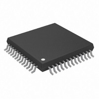
IC DAC 14BIT I2C 16CH 52-LQFP
Manufacturer
Analog Devices Inc
Specifications of AD5390BSTZ-5
Data Interface
I²C, Serial
Design Resources
8 to 16 Channels of Programmable Voltage with Excellent Temperature Drift Performance Using AD5390/1/2 (CN0029) AD5390/91/92 Channel Monitor Function (CN0030)
Settling Time
8µs
Number Of Bits
14
Number Of Converters
16
Voltage Supply Source
Single Supply
Power Dissipation (max)
35mW
Operating Temperature
-40°C ~ 85°C
Mounting Type
Surface Mount
Package / Case
52-LQFP
Resolution (bits)
14bit
Sampling Rate
125kSPS
Input Channel Type
Serial
Supply Voltage Range - Analogue
4.5V To 5.5V
Supply Voltage Range - Digital
2.7V To 5.5V
Lead Free Status / RoHS Status
Lead free / RoHS Compliant
For Use With
EVAL-AD5390EBZ - BOARD EVALUATION FOR AD5390
Lead Free Status / RoHS Status
Lead free / RoHS Compliant, Lead free / RoHS Compliant
Available stocks
Company
Part Number
Manufacturer
Quantity
Price
Company:

Part Number:
AD5390BSTZ-5
Manufacturer:
Analog Devices Inc
Quantity:
10 000


Power Amplifier Control
Multistage power amplifier designs require a large number of
setpoints in the operation and control of the output stage. The
AD539x are ideal for these applications because of their small
size (LFCSP package) and the integration of 8 and 16 channels,
offering 12- and 14-bit resolution. Figure 44 shows a typical
transmitter architecture, in which the AD539x DACs can be
used in the following control circuits: I
power control (APC), peak power control (PPC), transmit gain
control (TGC), and audio level control (ALC). DACs are also
required for variable voltage attenuators, phase shifter control,
and dc-setpoint control in the overall amplifier design.
Process Control Applications
The AD539x-5 family is ideal for process control applications
because it offers a combination of 8 and 16 channels and 12-bit
and 14-bit resolution. These applications generally require
output voltage ranges of 0 V to 5 V ±5 V, 0 V to 10 V ±10 V, and
current sink and source functions. The AD539x-5 products
operate from a single 5 V supply and, therefore, require external
signal conditioning to achieve the output ranges described here.
Figure 45 shows configurations to achieve these output ranges.
The key advantages of using AD539x products in these
applications are small package size, pin compatibility with the
ability to upgrade from 12 to 14 bits, integrated on-chip 2.5 V
reference with 10 ppm/°C maximum temperature coefficient,
and excellent accuracy specifications. The AD539x family
contains an offset and gain register for each channel, so users
can perform system-level calibration on a per-channel basis.
SOURCE
AUDIO
Figure 44. Multistage Power Amplifier Control
ALC
EXCITER
PPC
PHASE
SHIFT
AMPLIFIER
APC
POWER
BIAS
I
BIAS
control, average
TGC
LOAD
50Ω
Rev. A | Page 39 of 44
Optical Transceivers
The AD539x-3 family of products are ideally suited to optical
transceiver applications. In 300 pin MSA applications, for
example, digital-to-analog converters are required to control the
laser power, APD bias, modulator amplitude and diagnostic
information is required as analog outputs from the module. The
AD539x offering a combination of 8/16 channels, resolution of
12/14-bits in a 64 lead LFCSP package, operating from a supply
voltage of 2.7 V to 5.5 V supply with internal reference and
featuring I
component for use in these applications. Figure 46 shows a
typical configuration in an optical transceiver application.
RANGE
0V–10V
RANGE
±10V
PIN/APD
AND TIA
10G LDD
LASER
AND
1/4 OP4177
1/4 OP4177
1/4 OP747/
1/4 OP747/
IRXP
IMODMON
IMPD
IBIASMON
4R
R
2
C-compatible and SPI interface, make it an ideal
Figure 46. Optical Transceiver using the AD539x-3
BUS
I
Figure 45. Output Configurations for Process
3V
2
TIAs
C
4R
R
R
R
MUX
AIN
AV
DD
Control Applications
VOUT 3
VOUT 4
AD7994
CONTROLLER
SDA
AD539x-5
REFERENCE
AD5390/AD5391/AD5392
12-BIT
ADC
REFIN
2.5V
SCL
VOUT 0
VOUT 1
VOUT 2
0.1µF
SDA
SCL
REFOUT/REFIN
AD539x-3
DV
DD
AV
1/4 OP4177
1/4 OP747/
R
R
DD
VLSRBIAS
VLSRPWRMON
VXLOPMON
I
IMOD
2R
BIAS
2R
1/4 OP4177
1/4 OP747/
I SINK
R1
RANGE
RANGE
0V–5V
±5V
Related parts for AD5390BSTZ-5
Image
Part Number
Description
Manufacturer
Datasheet
Request
R

Part Number:
Description:
Wideband Dual-Channel Linear Multiplier/Divider
Manufacturer:
AD [Analog Devices]
Datasheet:

Part Number:
Description:
±1.7g Dual-Axis IMEMS Accelerometer Evaluation Board
Manufacturer:
Analog Devices Inc
Datasheet:

Part Number:
Description:
Inertial Sensor Evaluation System
Manufacturer:
Analog Devices Inc
Datasheet:
Part Number:
Description:
Manufacturer:
Analog Devices Inc
Datasheet:
Part Number:
Description:
Manufacturer:
Analog Devices Inc
Datasheet:
Part Number:
Description:
Manufacturer:
Analog Devices Inc
Datasheet:
Part Number:
Description:
Manufacturer:
Analog Devices Inc
Datasheet:
Part Number:
Description:
Manufacturer:
Analog Devices Inc
Datasheet:
Part Number:
Description:
Manufacturer:
Analog Devices Inc
Datasheet:
Part Number:
Description:
Manufacturer:
Analog Devices Inc
Datasheet:
Part Number:
Description:
Manufacturer:
Analog Devices Inc
Datasheet:
Part Number:
Description:
Manufacturer:
Analog Devices Inc
Datasheet:
Part Number:
Description:
Manufacturer:
Analog Devices Inc
Datasheet: