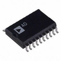
AD7302BR Analog Devices Inc, AD7302BR Datasheet - Page 11

AD7302BR
Manufacturer Part Number
AD7302BR
Description
IC DAC 8BIT DUAL 2.7V 20-SOIC
Manufacturer
Analog Devices Inc
Datasheet
1.AD7302BRUZ.pdf
(16 pages)
Specifications of AD7302BR
Mounting Type
Surface Mount
Rohs Status
RoHS non-compliant
Settling Time
1.2µs
Number Of Bits
8
Data Interface
Parallel
Number Of Converters
2
Voltage Supply Source
Single Supply
Power Dissipation (max)
24.8mW
Operating Temperature
-40°C ~ 105°C
Package / Case
20-SOIC (7.5mm Width)
Resolution (bits)
8bit
No. Of Pins
20
Update Rate
0.833MSPS
Peak Reflow Compatible (260 C)
No
Supply Voltage
5.5V
No. Of Bits
8 Bit
Leaded Process Compatible
No
Lead Free Status / RoHS Status
Contains lead / RoHS non-compliant
Available stocks
Company
Part Number
Manufacturer
Quantity
Price
Part Number:
AD7302BR
Manufacturer:
ADI/亚德诺
Quantity:
20 000
Company:
Part Number:
AD7302BRU
Manufacturer:
AD
Quantity:
4 130
Part Number:
AD7302BRUZ
Manufacturer:
ADI/亚德诺
Quantity:
20 000
Company:
Part Number:
AD7302BRZ
Manufacturer:
Maxim
Quantity:
25
Part Number:
AD7302BRZ
Manufacturer:
ADI/亚德诺
Quantity:
20 000
Part Number:
AD7302BRZ-REEL
Manufacturer:
ADI/亚德诺
Quantity:
20 000
Figure 27 shows a typical setup for the AD7302 when using its
internal reference. The internal reference is selected by tying the
REFIN pin to V
reference detect circuit that will select the internal V
on the voltage connected to the REFIN pin. If REFIN is within
a threshold voltage of a PMOS device (approximately 1 V) of
V
is more than 1 V below V
this pin is used as the reference for the DAC. The internal
reference on the AD7302 is V
converter within the AD7302 provides a gain of two. Thus the
output range of the DAC is from 0 V to V
REV. 0
V
DD
REF
the internal reference is selected. When the REFIN voltage
DAC INPUT
Table I. Output Voltage for Selected Input Codes
CODE
is the voltage applied to the external REFIN pin when
the external reference is selected and is V
internal reference is used.
Digital Input
MSB . . . LSB
1111 1111
1111 1110
1000 0001
1000 0000
0111 1111
0000 0001
0000 0000
2.V
V
REF
REF
Figure 26. DAC Transfer Function
0
00
DD
. Internally in the reference section there is a
01
DD
, the externally applied voltage at
DD
/2, the output current to voltage
Analog Output
2
2
2
V
2
2
0 V
7F
REF
255/256 V
254/256 V
129/256 V
127/256 V
V
80
V
REF
/256 V
81
DD
, based on Table I.
REF
REF
REF
REF
DD
/2 if the
DD
V
V
V
V
FE
/2 based
FF
–11–
Figure 27. Typical Configuration Selecting the Internal
Reference
Figure 28 shows a typical setup for the AD7302 when using an
external reference. The reference range for the AD7302 is from
1 V to V
but will saturate the output at both the top and bottom end of
the transfer function. There is a gain of two from input to output
on the AD7302. Suitable references for 5 V operation are the
AD780 and REF192. For 3 V operation a suitable external
reference would be the AD589 a 1.23 V bandgap reference.
Figure 28. Typical Configuration Using An External
Reference
AD589 WITH V
EXT REF
AD780/REF192
WITH V
DD
GND
OR
V
/2 V. Higher values of reference can be incorporated,
DD
IN
V
DD
= 5V
V
DD
OUT
= 3V
DATA BUS
0.1µF
REF IN
CLR
PD
D7–D0
0.1µF
V
DD
10µF
V
DD
AD7302
CONTROL INPUTS
= 3 TO 5V
0.1µF
DATA BUS
A/B
V
CLR
PD
REF IN
DD
D7–D0
CS
10µF
AGND DGND
V
WR LDAC
DD
AD7302
= 3 TO 5V
CONTROL INPUTS
V
V
V
A/B
OUT
OUT
DD
A
B
CS
AGND DGND
WR LDAC
AD7302
V
V
V
V
OUT
OUT
OUT
OUT
A
B
A
B
V
V
OUT
OUT
A
B


