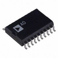
AD7305BR Analog Devices Inc, AD7305BR Datasheet - Page 7

AD7305BR
Manufacturer Part Number
AD7305BR
Description
IC DAC 8BIT QUAD 5V R-R 20-SOIC
Manufacturer
Analog Devices Inc
Specifications of AD7305BR
Mounting Type
Surface Mount
Rohs Status
RoHS non-compliant
Settling Time
1µs
Number Of Bits
8
Data Interface
Parallel
Number Of Converters
4
Voltage Supply Source
Dual ±
Power Dissipation (max)
60mW
Operating Temperature
-40°C ~ 85°C
Package / Case
20-SOIC (7.5mm Width)
Resolution (bits)
8bit
No. Of Pins
20
Peak Reflow Compatible (260 C)
No
Update Rate
1MSPS
No. Of Bits
8 Bit
Leaded Process Compatible
No
Interface Type
Parallel
Converter Type
Digital to Analog
Current, Output
±3 mA (Typ.)
Input Capacitance
8 pF (Max.)
Number Of Converter
4
Number Of Pins
20
Package Type
SOIC
Power Dissipation
15 mW (Max.)
Resolution
8 Bits
Slew Rate
1⁄2.7 V⁄uS
Temperature, Operating, Maximum
85 °C
Temperature, Operating, Minimum
-40 °C
Thermal Resistance, Junction To Ambient
74 °C⁄W
Voltage, Input, High Level
2.1 V (Max.)
Voltage, Input, Low Level
0.6 V (Min.)
Voltage, Range
2.7 to 5.5 V
Lead Free Status / RoHS Status
Contains lead / RoHS non-compliant
Available stocks
Company
Part Number
Manufacturer
Quantity
Price
Company:
Part Number:
AD7305BR
Manufacturer:
AD
Quantity:
5 510
Part Number:
AD7305BRUZ
Manufacturer:
ADI/亚德诺
Quantity:
20 000
Part Number:
AD7305BRZ
Manufacturer:
AD
Quantity:
20 000
Part Number:
AD7305BRZ-REEL
Manufacturer:
ADI/亚德诺
Quantity:
20 000
Table 6. AD7305 Control Logic Truth Table
WR
L
↑+
L
↑+
L
↑+
L
↑+
H
L
H
H
1
2
↑+ positive logic transition; ↓– negative logic transition; X don’t care.
LDAC is a level-sensitive input.
1
A1
L
L
L
L
H
H
H
H
X
X
X
X
A0
L
L
H
H
L
L
H
H
X
X
X
X
LDAC
H
H
H
H
H
H
H
H
L
L
↑+
H
2
Input Register Function
Register A loaded with DB0 to DB7
Register A latched with DB0 to DB7
Register B loaded with DB0 to DB7
Register B latched with DB0 to DB7
Register C loaded with DB0 to DB7
Register C latched with DB0 to DB7
Register D loaded with DB0 to DB7
Register D latched with DB0 to DB7
No effect
Input register x transparent to DB0 to DB7
No effect
No effect, device not selected
A0/SHDN
I
DD
D0–D7
A0, A1
LDAC
V
OUT
WR
Figure 7. AD7305 Timing Diagram Zoom In
Figure 6. AD7305 General Timing Diagram
t
Rev. C | Page 7 of 20
SDN
t
t
WR
LS
t
t
AS
DS
t
S
t
t
t
AH
DH
LH
DAC Register Function
Latched with previous contents, no change
Latched with previous contents, no change
Latched with previous contents, no change
Latched with previous contents, no change
Latched with previous contents, no change
Latched with previous contents, no change
Latched with previous contents, no change
Latched with previous contents, no change
All input register contents loaded, register transparent
Register transparent
All input register contents latched
No effect, device not selected
ERROR BAND
±1 LSB
t
t
SDR
LDW
AD7304/AD7305


