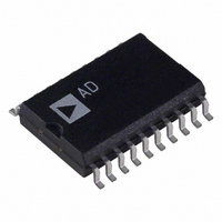
AD7305BR Analog Devices Inc, AD7305BR Datasheet - Page 9

AD7305BR
Manufacturer Part Number
AD7305BR
Description
IC DAC 8BIT QUAD 5V R-R 20-SOIC
Manufacturer
Analog Devices Inc
Specifications of AD7305BR
Mounting Type
Surface Mount
Rohs Status
RoHS non-compliant
Settling Time
1µs
Number Of Bits
8
Data Interface
Parallel
Number Of Converters
4
Voltage Supply Source
Dual ±
Power Dissipation (max)
60mW
Operating Temperature
-40°C ~ 85°C
Package / Case
20-SOIC (7.5mm Width)
Resolution (bits)
8bit
No. Of Pins
20
Peak Reflow Compatible (260 C)
No
Update Rate
1MSPS
No. Of Bits
8 Bit
Leaded Process Compatible
No
Interface Type
Parallel
Converter Type
Digital to Analog
Current, Output
±3 mA (Typ.)
Input Capacitance
8 pF (Max.)
Number Of Converter
4
Number Of Pins
20
Package Type
SOIC
Power Dissipation
15 mW (Max.)
Resolution
8 Bits
Slew Rate
1⁄2.7 V⁄uS
Temperature, Operating, Maximum
85 °C
Temperature, Operating, Minimum
-40 °C
Thermal Resistance, Junction To Ambient
74 °C⁄W
Voltage, Input, High Level
2.1 V (Max.)
Voltage, Input, Low Level
0.6 V (Min.)
Voltage, Range
2.7 to 5.5 V
Lead Free Status / RoHS Status
Contains lead / RoHS non-compliant
Available stocks
Company
Part Number
Manufacturer
Quantity
Price
Company:
Part Number:
AD7305BR
Manufacturer:
AD
Quantity:
5 510
Part Number:
AD7305BRUZ
Manufacturer:
ADI/亚德诺
Quantity:
20 000
Part Number:
AD7305BRZ
Manufacturer:
AD
Quantity:
20 000
Part Number:
AD7305BRZ-REEL
Manufacturer:
ADI/亚德诺
Quantity:
20 000
Table 8. AD7305 Pin Function Description
Pin No.
1
2
3
4
5
6
7
8
9
10
11
12
13
14
15
16
17
18
19
20
Mnemonic
V
V
V
V
GND
LDAC
DB7
DB6
DB5
DB4
DB3
DB2
DB1
DB0
WR
A1
A0/SHDN
V
V
V
OUT
OUT
SS
REF
DD
OUT
OUT
B
A
D
C
Description
Channel B Rail-to-Rail Buffered DAC Voltage Output. Full-scale set by reference voltage applied to V
open circuit when SHDN is enabled.
Channel A Rail-to-Rail Buffered DAC Voltage Output. Full-scale set by reference voltage applied to V
open circuit when SHDN is enabled.
Negative Power Supply Input. Specified range of operation is 0 V to –5.5 V.
Channel B Reference Input. Establishes V
Common Analog and Digital Ground.
Load DAC Register Strobe, Active Low. Simultaneously transfers data from all four input registers into the
corresponding DAC registers. Asynchronous active low input. DAC register is transparent when LDAC = 0. See Table 6
for operation.
MSB Digital Input Data Bit.
Data Bit 6.
Data Bit 5.
Data Bit 4.
Data Bit 3.
Data Bit 2.
Data Bit 1.
LSB Digital Input Data Bit.
Write Data into Input Register Control Line, Active Low. See Table 6 for operation.
Address Bit 1.
Address Bit 0/Hardware Shutdown (SHDN) Control Input, Active When Pin Is Left Floating by a Three-State Logic
Driver. Does not effect DAC register contents as long as power is present on V
Positive Power Supply Input. Specified range of operation is 2.7 V to 5.5 V.
Channel D Rail-to-Rail Buffered DAC Voltage Output. Full-scale set by reference voltage applied to V
open circuit when SHDN is enabled.
Channel C Rail-to-Rail Buffered DAC Voltage Output. Full-scale set by reference voltage applied to V
open circuit when SHDN is enabled.
V
V
LDAC
OUT
OUT
V
GND
DB7
DB6
DB5
DB4
Figure 9. AD7305 Pin Configuration
V
REF
SS
B
A
10
1
2
3
4
5
6
7
8
9
Rev. C | Page 9 of 20
(Not to Scale)
AD7305
TOP VIEW
OUT
full-scale voltage. Specified range of operation is V
20
19
18
17
16
15
14
13
12
11
V
V
V
A0/SHDN
A1
WR
DB0
DB1
DB2
DB3
OUT
OUT
DD
C
D
DD
.
AD7304/AD7305
SS
< V
REF
REF
REF
REF
REF
B pin. Output is
A pin. Output is
C pin. Output is
D pin. Output is
< V
DD
.


