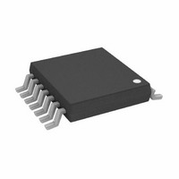
AD5666BRUZ-1 Analog Devices Inc, AD5666BRUZ-1 Datasheet - Page 11

AD5666BRUZ-1
Manufacturer Part Number
AD5666BRUZ-1
Description
IC DAC 16BIT QUAD 3V 14-TSSOP
Manufacturer
Analog Devices Inc
Datasheet
1.AD5666ARUZ-2REEL7.pdf
(28 pages)
Specifications of AD5666BRUZ-1
Data Interface
DSP, MICROWIRE™, QSPI™, Serial, SPI™
Settling Time
6µs
Number Of Bits
16
Number Of Converters
4
Voltage Supply Source
Single Supply
Operating Temperature
-40°C ~ 105°C
Mounting Type
Surface Mount
Package / Case
14-TSSOP
Resolution (bits)
16bit
Sampling Rate
95kSPS
Input Channel Type
Serial
Supply Voltage Range - Analogue
2.7V To 3.6V, 4.5V To 5.5V
Supply Current
1.3mA
Digital Ic
RoHS Compliant
Lead Free Status / RoHS Status
Lead free / RoHS Compliant
Power Dissipation (max)
-
Lead Free Status / RoHS Status
Lead free / RoHS Compliant
Available stocks
Company
Part Number
Manufacturer
Quantity
Price
Part Number:
AD5666BRUZ-1
Manufacturer:
ADI/亚德诺
Quantity:
20 000
Company:
Part Number:
AD5666BRUZ-1REEL7
Manufacturer:
AOS
Quantity:
43 000
PIN CONFIGURATION AND FUNCTION DESCRIPTIONS
Table 6. Pin Function Descriptions
Pin No.
1
2
3
4
5
6
7
8
9
10
11
12
13
14
SDO
DIN
Mnemonic
LDAC
SYNC
V
V
V
POR
V
CLR
V
V
GND
SCLK
DD
OUT
OUT
REFIN
OUT
OUT
A
C
D
B
/V
REFOUT
Description
Pulsing this pin low allows any or all DAC registers to be updated if the input registers have new data.
This allows all DAC outputs to simultaneously update. Alternatively, this pin can be tied permanently low.
Active Low Control Input. This is the frame synchronization signal for the input data. When SYNC goes
low, it powers on the SCLK and DIN buffers and enables the input shift register. Data is transferred in
on the falling edges of the next 32 clocks. If SYNC is taken high before the 32
edge of SYNC acts as an interrupt and the write sequence is ignored by the device.
Power Supply Input. These parts can be operated from 2.7 V to 5.5 V, and the supply should be decoupled
with a 10 μF capacitor in parallel with a 0.1 μF capacitor to GND.
Analog Output Voltage from DAC A. The output amplifier has rail-to-rail operation.
Analog Output Voltage from DAC C. The output amplifier has rail-to-rail operation.
Power-on Reset Pin. Tying this pin to GND powers up the part to 0 V. Tying this pin to V
the part to midscale.
The AD5666 has a common pin for reference input and reference output. When using the internal
reference, this is the reference output pin. When using an external reference, this is the reference input
pin. The default for this pin is as a reference input.
Serial Data Output. Can be used for daisy-chaining a number of these devices together or for reading
back the data in the shift register for diagnostic purposes. The serial data is transferred on the rising edge
of SCLK and is valid on the falling edge of the clock.
Asynchronous Clear Input. The CLR input is falling edge sensitive. When CLR is low, all LDAC pulses are
ignored. When CLR is activated, the input register and the DAC register are updated with the data
contained in the CLR code register—zero, midscale, or full scale. Default setting clears the output to 0 V.
Analog Output Voltage from DAC D. The output amplifier has rail-to-rail operation.
Analog Output Voltage from DAC B. The output amplifier has rail-to-rail operation.
Ground Reference Point for All Circuitry on the Part.
Serial Data Input. This device has a 32-bit shift register. Data is clocked into the register on the falling
edge of the serial clock input.
Serial Clock Input. Data is clocked into the input shift register on the falling edge of the serial clock input.
Data can be transferred at rates of up to 50 MHz.
V
REFIN
/V
Figure 5. 14-Lead TSSOP (RU-14)
REFOUT
V
V
LDAC
SYNC
OUT
OUT
POR
V
DD
Rev. D | Page 11 of 28
C
A
1
2
3
4
5
6
7
(Not to Scale)
TOP VIEW
AD5666
13
12
11
10
14
9
8
SCLK
DIN
GND
V
V
SDO
CLR
OUT
OUT
B
D
nd
falling edge, the rising
DD
powers up
AD5666


