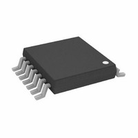
AD5666BRUZ-1 Analog Devices Inc, AD5666BRUZ-1 Datasheet - Page 8

AD5666BRUZ-1
Manufacturer Part Number
AD5666BRUZ-1
Description
IC DAC 16BIT QUAD 3V 14-TSSOP
Manufacturer
Analog Devices Inc
Datasheet
1.AD5666ARUZ-2REEL7.pdf
(28 pages)
Specifications of AD5666BRUZ-1
Data Interface
DSP, MICROWIRE™, QSPI™, Serial, SPI™
Settling Time
6µs
Number Of Bits
16
Number Of Converters
4
Voltage Supply Source
Single Supply
Operating Temperature
-40°C ~ 105°C
Mounting Type
Surface Mount
Package / Case
14-TSSOP
Resolution (bits)
16bit
Sampling Rate
95kSPS
Input Channel Type
Serial
Supply Voltage Range - Analogue
2.7V To 3.6V, 4.5V To 5.5V
Supply Current
1.3mA
Digital Ic
RoHS Compliant
Lead Free Status / RoHS Status
Lead free / RoHS Compliant
Power Dissipation (max)
-
Lead Free Status / RoHS Status
Lead free / RoHS Compliant
Available stocks
Company
Part Number
Manufacturer
Quantity
Price
Part Number:
AD5666BRUZ-1
Manufacturer:
ADI/亚德诺
Quantity:
20 000
Company:
Part Number:
AD5666BRUZ-1REEL7
Manufacturer:
AOS
Quantity:
43 000
AD5666
TIMING CHARACTERISTICS
All input signals are specified with tr = tf = 1 ns/V (10% to 90% of V
Figure 5. V
Table 4.
Parameter
t
t
t
t
t
t
t
t
t
t
t
t
t
t
t
t
t
t
t
1
2
3
1
2
3
4
5
6
7
8
9
10
11
12
13
14
15
16
17
18
19
Maximum SCLK frequency is 50 MHz at V
Measured with the load circuit of Figure 16. t
Daisy-chain mode only.
1
3
3
3
2, 3
DD
= 2.7 V to 5.5 V. All specifications T
Limit at T
V
20
8
8
13
4
4
0
15
13
0
10
15
5
0
300
22
5
8
0
DD
= 2.7 V to 5.5 V
MIN
DD
, T
= 2.7 V to 5.5 V. Guaranteed by design and characterization; not production tested.
16
MAX
determines the maximum SCLK frequency in daisy-chain mode.
Figure 2. Load Circuit for Digital Output (SDO) Timing Specifications
TO OUTPUT
MIN
to T
PIN
MAX
50pF
Unit
ns min
ns min
ns min
ns min
ns min
ns min
ns min
ns min
ns min
ns min
ns min
ns min
ns min
ns min
ns typ
ns max
ns min
ns min
ns min
C
, unless otherwise noted.
Rev. D | Page 8 of 28
L
2mA
2mA
DD
) and timed from a voltage level of (V
I
I
OL
OH
Conditions/Comments
SCLK cycle time
SCLK high time
SCLK low time
SYNC to SCLK falling edge set-up time
Data set-up time
Data hold time
SCLK falling edge to SYNC rising edge
Minimum SYNC high time
SYNC rising edge to SCLK fall ignore
SCLK falling edge to SYNC fall ignore
LDAC pulse width low
SCLK falling edge to LDAC rising edge
CLR pulse width low
SCLK falling edge to LDAC falling edge
CLR pulse activation time
SCLK rising edge to SDO valid
SCLK falling edge to SYNC rising edge
SYNC rising edge to SCLK rising edge
SYNC rising edge to LDAC falling edge
V
OH
(MIN)
IL
+ V
IH
)/2. See Figure 3 and


