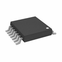
AD5666BRUZ-1 Analog Devices Inc, AD5666BRUZ-1 Datasheet - Page 21

AD5666BRUZ-1
Manufacturer Part Number
AD5666BRUZ-1
Description
IC DAC 16BIT QUAD 3V 14-TSSOP
Manufacturer
Analog Devices Inc
Datasheet
1.AD5666ARUZ-2REEL7.pdf
(28 pages)
Specifications of AD5666BRUZ-1
Data Interface
DSP, MICROWIRE™, QSPI™, Serial, SPI™
Settling Time
6µs
Number Of Bits
16
Number Of Converters
4
Voltage Supply Source
Single Supply
Operating Temperature
-40°C ~ 105°C
Mounting Type
Surface Mount
Package / Case
14-TSSOP
Resolution (bits)
16bit
Sampling Rate
95kSPS
Input Channel Type
Serial
Supply Voltage Range - Analogue
2.7V To 3.6V, 4.5V To 5.5V
Supply Current
1.3mA
Digital Ic
RoHS Compliant
Lead Free Status / RoHS Status
Lead free / RoHS Compliant
Power Dissipation (max)
-
Lead Free Status / RoHS Status
Lead free / RoHS Compliant
Available stocks
Company
Part Number
Manufacturer
Quantity
Price
Part Number:
AD5666BRUZ-1
Manufacturer:
ADI/亚德诺
Quantity:
20 000
Company:
Part Number:
AD5666BRUZ-1REEL7
Manufacturer:
AOS
Quantity:
43 000
OUTPUT AMPLIFIER
The output buffer amplifier can generate rail-to-rail voltages on
its output, which gives an output range of 0 V to V
amplifier is capable of driving a load of 2 kΩ in parallel with
1000 pF to GND. The source and sink capabilities of the output
amplifier can be seen in Figure 19 and Figure 20. The slew rate
is 1.5 V/μs with a ¼ to ¾ scale settling time of 10 μs.
SERIAL INTERFACE
The AD5666 has a 3-wire serial interface ( SYNC , SCLK, and
DIN) that is compatible with SPI, QSPI, and MICROWIRE
interface standards as well as most DSPs. See
timing diagram of a typical write sequence.
The write sequence begins by bringing the SYNC line low. Data
from the DIN line is clocked into the 32-bit shift register on the
falling edge of SCLK. The serial clock frequency can be as high
as 50 MHz, making the AD5666 compatible with high speed
DSPs. On the 32
in and the programmed function is executed, that is, a change
in DAC register contents and/or a change in the mode of
operation. At this stage, the SYNC line can be kept low or be
brought high. In either case, it must be brought high for a
minimum of 15 ns before the next write sequence so that a
falling edge of SYNC can initiate the next write sequence.
Because the SYNC buffer draws more current when V
than it does when V
between write sequences for even lower power operation of the
part. As is mentioned previously, however, SYNC must be
brought high again just before the next write sequence.
nd
falling clock edge, the last data bit is clocked
IN
= 0.8 V, SYNC should be idled low
Figure 3
DD
. The
for a
IN
= 2 V
Rev. D | Page 21 of 28
Table 7. Command Definitions
C3
0
0
0
0
0
0
0
0
1
1
–
1
Table 8. Address Commands
A3
0
0
0
0
1
Command
C2
0
0
0
0
1
1
1
1
0
0
–
1
C1
0
0
1
1
0
0
1
1
0
0
–
1
A2
0
0
0
0
1
Address (n)
C0
0
1
0
1
0
1
0
1
0
1
–
1
Description
Write to Input Register n
Update DAC Register n
Write to Input Register n, update all
(software LDAC)
Write to and update DAC Channel n
Power down/power up DAC
Load clear code register
Load LDAC register
Reset (power-on reset)
Set up DCEN/REF register
No operation
Reserved
Reserved
A1
0
0
1
1
1
A0
0
1
0
1
1
Selected DAC
Channel
DAC A
DAC B
DAC C
DAC D
All DACs
AD5666


