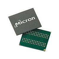
MT46H16M32LFCM-6 AT:B Micron Technology Inc, MT46H16M32LFCM-6 AT:B Datasheet - Page 63

MT46H16M32LFCM-6 AT:B
Manufacturer Part Number
MT46H16M32LFCM-6 AT:B
Description
Manufacturer
Micron Technology Inc
Type
DDR SDRAMr
Datasheet
1.MT46H16M32LFCM-6_ATB.pdf
(98 pages)
Specifications of MT46H16M32LFCM-6 AT:B
Organization
16Mx32
Density
512Mb
Address Bus
15b
Access Time (max)
6.5/5ns
Maximum Clock Rate
166MHz
Operating Supply Voltage (typ)
1.8V
Package Type
VFBGA
Operating Temp Range
0C to 70C
Operating Supply Voltage (max)
1.95V
Operating Supply Voltage (min)
1.7V
Supply Current
115mA
Pin Count
90
Mounting
Surface Mount
Operating Temperature Classification
Commercial
Lead Free Status / Rohs Status
Compliant
- Current page: 63 of 98
- Download datasheet (4Mb)
Figure 25: Nonconsecutive READ Bursts
PDF: 09005aef82d5d305
512mb_ddr_mobile_sdram_t47m.pdf – Rev. I 12/09 EN
Command
Command
Address
Address
DQS
DQS
CK#
CK#
DQ
DQ
CK
CK
Notes:
READ
Bank,
READ
Bank,
Col n
Col n
T0
T0
1. D
2. BL = 4, 8, or 16 (if burst is 8 or 16, the second burst interrupts the first).
3. Shown with nominal
4. Example applies when READ commands are issued to different devices or nonconsecu-
tive READs.
OUT
CL = 2
NOP
NOP
T1
T1
n (or b) = data-out from column n (or column b).
CL = 3
T1n
T1n
D
OUT
NOP
NOP
T2
T2
1
t
AC,
D
OUT
T2n
T2n
63
t
DQSCK, and
D
512Mb: x16, x32 Mobile LPDDR SDRAM
D
OUT
READ
Bank,
READ
Bank,
Col b
Col b
OUT
T3
T3
Micron Technology, Inc. reserves the right to change products or specifications without notice.
D
D
T3n
T3n
t
OUT
DQSQ.
OUT
CL = 2
D
T4
T4
NOP
NOP
OUT
Don’t Care
CL = 3
D
T4n
T4n
OUT
© 2004 Micron Technology, Inc. All rights reserved.
T5
T5
NOP
NOP
D
OUT
READ Operation
Transitioning Data
T5n
T5n
D
OUT
T6
T6
NOP
NOP
D
D
OUT
OUT
Related parts for MT46H16M32LFCM-6 AT:B
Image
Part Number
Description
Manufacturer
Datasheet
Request
R

Part Number:
Description:
IC SDRAM 64MBIT 133MHZ 54TSOP
Manufacturer:
Micron Technology Inc
Datasheet:

Part Number:
Description:
IC SDRAM 64MBIT 5.5NS 86TSOP
Manufacturer:
Micron Technology Inc
Datasheet:

Part Number:
Description:
IC SDRAM 64MBIT 200MHZ 86TSOP
Manufacturer:
Micron Technology Inc
Datasheet:

Part Number:
Description:
IC SDRAM 64MBIT 133MHZ 54TSOP
Manufacturer:
Micron Technology Inc
Datasheet:

Part Number:
Description:
IC SDRAM 128MBIT 133MHZ 54TSOP
Manufacturer:
Micron Technology Inc
Datasheet:

Part Number:
Description:
IC SDRAM 256MBIT 133MHZ 90VFBGA
Manufacturer:
Micron Technology Inc
Datasheet:

Part Number:
Description:
IC SDRAM 128MBIT 133MHZ 54TSOP
Manufacturer:
Micron Technology Inc
Datasheet:

Part Number:
Description:
IC SDRAM 256MBIT 133MHZ 54TSOP
Manufacturer:
Micron Technology Inc
Datasheet:

Part Number:
Description:
IC DDR SDRAM 512MBIT 6NS 66TSOP
Manufacturer:
Micron Technology Inc
Datasheet:

Part Number:
Description:
IC SDRAM 128MBIT 167MHZ 86TSOP
Manufacturer:
Micron Technology Inc
Datasheet:

Part Number:
Description:
IC SDRAM 128MBIT 143MHZ 86TSOP
Manufacturer:
Micron Technology Inc
Datasheet:

Part Number:
Description:
SDRAM 256M-BIT 1.8V 54-PIN VFBGA
Manufacturer:
Micron Technology Inc
Datasheet:

Part Number:
Description:
IC SDRAM 128MBIT 143MHZ 86TSOP
Manufacturer:
Micron Technology Inc
Datasheet:

Part Number:
Description:
IC SDRAM 128MBIT 125MHZ 54VFBGA
Manufacturer:
Micron Technology Inc
Datasheet:

Part Number:
Description:
IC SDRAM 128MBIT 125MHZ 54VFBGA
Manufacturer:
Micron Technology Inc
Datasheet:


