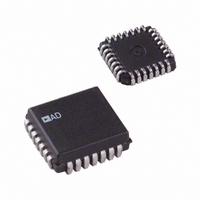
AD7846JP Analog Devices Inc, AD7846JP Datasheet - Page 14

AD7846JP
Manufacturer Part Number
AD7846JP
Description
IC DAC 16BIT LC2MOS VOUT 28PLCC
Manufacturer
Analog Devices Inc
Datasheet
1.AD7846JPZ.pdf
(24 pages)
Specifications of AD7846JP
Data Interface
Parallel
Rohs Status
RoHS non-compliant
Settling Time
7µs
Number Of Bits
16
Number Of Converters
1
Voltage Supply Source
Dual ±
Power Dissipation (max)
100mW
Operating Temperature
0°C ~ 70°C
Mounting Type
Surface Mount
Package / Case
28-LCC (J-Lead)
Resolution (bits)
16bit
Sampling Rate
143kSPS
Input Channel Type
Parallel
Supply Voltage Range - Digital
4.75V To 5.25V
Supply Current
5mA
Digital Ic Case Style
LCC
Lead Free Status / RoHS Status
Contains lead / RoHS non-compliant
Available stocks
Company
Part Number
Manufacturer
Quantity
Price
Company:
Part Number:
AD7846JP
Manufacturer:
AD
Quantity:
1 980
Company:
Part Number:
AD7846JP
Manufacturer:
AD
Quantity:
5 510
Part Number:
AD7846JP
Manufacturer:
ADI/亚德诺
Quantity:
20 000
Company:
Part Number:
AD7846JP-REEL
Manufacturer:
AD
Quantity:
5 510
Company:
Part Number:
AD7846JP-REEL
Manufacturer:
LT
Quantity:
5 510
Company:
Part Number:
AD7846JP-REEL
Manufacturer:
Analog Devices Inc
Quantity:
10 000
Company:
Part Number:
AD7846JPZ
Manufacturer:
Analog Devices Inc
Quantity:
10 000
Part Number:
AD7846JPZ
Manufacturer:
ADI/亚德诺
Quantity:
20 000
Company:
Part Number:
AD7846JPZ-REEL
Manufacturer:
Analog Devices Inc
Quantity:
10 000
AD7846
BIPOLAR OPERATION
Figure 24 shows the AD7846 set up for ±10 V bipolar operation.
The AD588 provides precision ±5 V tracking outputs that are
fed to the V
for Figure 24 is shown in Table 9.
Table 9. Offset Binary Code Table for Figure 24
Binary Number in DAC Latch
MSB
1111 1111 1111 1111
1000 0000 0000 0001
1000 0000 0000 0000
0111 1111 1111 1111
0000 0000 0000 0000
1
10kΩ
*ADDITIONAL PINS OMITTED FOR CLARITY
LSB = 10 V/2
R2
100kΩ
R3
1µF
C1
15
REF+
= 10 V/32,768 = 305 μV.
10
11
7
9
5
and V
12
AD588
Figure 24. Bipolar ±10 V Operation
4
LSB
+15V
8
REF−
6
13
1
R1
39kΩ
14
15
16
2
3
1
inputs of the AD7846. The code table
+15V
–15V
7
8
V
V
Analog Output (V
+10 (32,767/32,768) V
+10 (1/32,768) V
0 V
−10 (1/32,768) V
−10 (32,768/32,768) V
+15V
REF+
REF–
V
AD7846*
4
DD
–15V
V
SS
9
DGND
V
+5V
V
21
OUT
R
CC
IN
20
5
6
V
(–10V TO +10V)
SIGNAL
GROUND
OUT
OUT
)
Rev. G | Page 14 of 24
Full-scale and bipolar zero adjustment are provided by varying
the gain and balance on the AD588. R2 varies the gain on the
AD588 while R3 adjusts the +5 V and −5 V outputs together
with respect to ground.
For bipolar zero adjustment on the AD7846, load the DAC with
100…000 and adjust R3 until V
by loading the DAC with all 1s and adjusting R2 until V
9.999694 V.
When bipolar zero and full-scale adjustment are not needed, R2
and R3 can be omitted, Pin 12 on the AD588 should be connected
to Pin 11, and Pin 5 should be left floating. If a user wants a 5 V
output range, there are two choices. By tying Pin 6 (R
AD7846 to V
unity and the output range is ±5 V. If only a positive 5 V reference
is available, bipolar ±5 V operation is still possible. Tie V
0 V and connect R
range. However, the linearity, gain, and offset error specifications
are the same as the unipolar 0 V to 5 V range.
MULTIPLYING OPERATION
The AD7846 is a full multiplying DAC. To obtain four-quadrant
multiplication, tie V
tie R
response when the DAC is used in this fashion.
IN
to V
REF+
OUT
. Figure 11 shows the large signal frequency
(Pin 5), the output stage gain is reduced to
IN
REF−
to V
to 0 V, apply the ac input to V
REF+
. This also gives a ±5 V output
OUT
= 0 V. Full scale is adjusted
IN
REF+
) of the
OUT
REF−
, and
=
to


