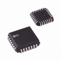
AD7846JP Analog Devices Inc, AD7846JP Datasheet - Page 4

AD7846JP
Manufacturer Part Number
AD7846JP
Description
IC DAC 16BIT LC2MOS VOUT 28PLCC
Manufacturer
Analog Devices Inc
Datasheet
1.AD7846JPZ.pdf
(24 pages)
Specifications of AD7846JP
Data Interface
Parallel
Rohs Status
RoHS non-compliant
Settling Time
7µs
Number Of Bits
16
Number Of Converters
1
Voltage Supply Source
Dual ±
Power Dissipation (max)
100mW
Operating Temperature
0°C ~ 70°C
Mounting Type
Surface Mount
Package / Case
28-LCC (J-Lead)
Resolution (bits)
16bit
Sampling Rate
143kSPS
Input Channel Type
Parallel
Supply Voltage Range - Digital
4.75V To 5.25V
Supply Current
5mA
Digital Ic Case Style
LCC
Lead Free Status / RoHS Status
Contains lead / RoHS non-compliant
Available stocks
Company
Part Number
Manufacturer
Quantity
Price
Company:
Part Number:
AD7846JP
Manufacturer:
AD
Quantity:
1 980
Company:
Part Number:
AD7846JP
Manufacturer:
AD
Quantity:
5 510
Part Number:
AD7846JP
Manufacturer:
ADI/亚德诺
Quantity:
20 000
Company:
Part Number:
AD7846JP-REEL
Manufacturer:
AD
Quantity:
5 510
Company:
Part Number:
AD7846JP-REEL
Manufacturer:
LT
Quantity:
5 510
Company:
Part Number:
AD7846JP-REEL
Manufacturer:
Analog Devices Inc
Quantity:
10 000
Company:
Part Number:
AD7846JPZ
Manufacturer:
Analog Devices Inc
Quantity:
10 000
Part Number:
AD7846JPZ
Manufacturer:
ADI/亚德诺
Quantity:
20 000
Company:
Part Number:
AD7846JPZ-REEL
Manufacturer:
Analog Devices Inc
Quantity:
10 000
AD7846
Parameter
DIGITAL OUTPUTS
POWER REQUIREMENTS
1
2
3
4
AC PERFORMANCE CHARACTERISTICS
These characteristics are included for design guidance and are not subject to test. V
to −15.75 V; V
Table 2.
Parameter
Output Settling Time
Slew Rate
Digital-to-Analog Glitch
Impulse
AC Feedthrough
Digital Feedthrough
Output Noise Voltage
1
Temperature ranges as follows: J, K versions: 0°C to +70°C; A, B versions: −40°C to +85°C.
Guaranteed by design and characterization, not production tested.
The AD7846 is functional with power supplies of ±12 V. See the Typical Performance Characteristics section.
Sensitivity of gain error, offset error, and bipolar zero error to V
LDAC = 0. Settling time does not include deglitching time of 2.5 μs (typ).
V
V
Floating State Leakage Current
Floating State Output Capacitance
V
V
V
I
I
I
Power Supply Sensitivity
Power Dissipation
Density, 1 kHz to 100 kHz
DD
SS
CC
OL
OH
DD
SS
CC
(Output Low Voltage)
(Output High Voltage)
1
CC
= +4.75 V to +5.25 V; R
1
3
4
Limit at T
6
9
7
70
0.5
10
50
2
MIN
IN
J, A Versions
0.4
4.0
±10
10
+11.4/+15.75
−11.4/−15.75
+4.75/+5.25
5
5
1
1.5
100
connected to 0 V, unless otherwise noted.
to T
MAX
(All Versions)
DD
, V
SS
variations.
K, B Versions
0.4
4.0
±10
10
+11.4/+15.75
−11.4/−15.75
+4.75/+5.25
5
5
1
1.5
100
Rev. G | Page 4 of 24
nV-sec typ
Unit
μs max
μs max
V/μs typ
nV-sec typ
mV p-p typ
nV/√Hz typ
Unit
V max
V min
μA max
pF max
V min/V max
V min/V max
V min/V max
mA max
mA max
mA max
LSB/V max
mW typ
Test Conditions/Comments
To 0.006% FSR, V
To 0.003% FSR, V
DAC alternately loaded with 10…0000 and 01…1111,
V
V
with all 0s
DAC alternately loaded with all 1s and all 0s. CS high
Measured at V
V
REF+
OUT
REF−
REF+
unloaded
= +5 V; V
= 0 V, V
= V
REF−
= 0 V
REF+
OUT
DD
= 1 V rms, 10 kHz sine wave, DAC loaded
Test Conditions/Comments
I
I
DB0 to DB15 = 0 to V
V
V
V
SINK
SOURCE
OUT
OUT
, DAC loaded with 0111011…11,
= +14.25 V to +15.75 V; V
OUT
OUT
OUT
loaded, V
loaded, V
= 1.6 mA
unloaded
unloaded
unloaded
= 400 μA
REF−
REF−
= 0 V, typically 3.5 μs
= –5 V, typically 6.5 μs
CC
SS
= −14.25 V


