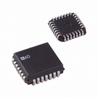
AD7846JP Analog Devices Inc, AD7846JP Datasheet - Page 16

AD7846JP
Manufacturer Part Number
AD7846JP
Description
IC DAC 16BIT LC2MOS VOUT 28PLCC
Manufacturer
Analog Devices Inc
Datasheet
1.AD7846JPZ.pdf
(24 pages)
Specifications of AD7846JP
Data Interface
Parallel
Rohs Status
RoHS non-compliant
Settling Time
7µs
Number Of Bits
16
Number Of Converters
1
Voltage Supply Source
Dual ±
Power Dissipation (max)
100mW
Operating Temperature
0°C ~ 70°C
Mounting Type
Surface Mount
Package / Case
28-LCC (J-Lead)
Resolution (bits)
16bit
Sampling Rate
143kSPS
Input Channel Type
Parallel
Supply Voltage Range - Digital
4.75V To 5.25V
Supply Current
5mA
Digital Ic Case Style
LCC
Lead Free Status / RoHS Status
Contains lead / RoHS non-compliant
Available stocks
Company
Part Number
Manufacturer
Quantity
Price
Company:
Part Number:
AD7846JP
Manufacturer:
AD
Quantity:
1 980
Company:
Part Number:
AD7846JP
Manufacturer:
AD
Quantity:
5 510
Part Number:
AD7846JP
Manufacturer:
ADI/亚德诺
Quantity:
20 000
Company:
Part Number:
AD7846JP-REEL
Manufacturer:
AD
Quantity:
5 510
Company:
Part Number:
AD7846JP-REEL
Manufacturer:
LT
Quantity:
5 510
Company:
Part Number:
AD7846JP-REEL
Manufacturer:
Analog Devices Inc
Quantity:
10 000
Company:
Part Number:
AD7846JPZ
Manufacturer:
Analog Devices Inc
Quantity:
10 000
Part Number:
AD7846JPZ
Manufacturer:
ADI/亚德诺
Quantity:
20 000
Company:
Part Number:
AD7846JPZ-REEL
Manufacturer:
Analog Devices Inc
Quantity:
10 000
AD7846
MICROPROCESSOR INTERFACING
AD7846-TO-8086 INTERFACE
Figure 26 shows the 8086 16-bit processor interfacing to the
AD7846. The double buffering feature of the DAC is not used in
this circuit because LDAC is permanently tied to 0 V. AD0 to
AD15 (the 16-bit data bus) are connected to the DAC data bus
(DB0 to DB15). The 16-bit word is written to the DAC in one
MOV instruction and the analog output responds immediately.
In this example, the DAC address is 0xD000.
In a multiple DAC system, the double buffering of the AD7846
allows the user to simultaneously update all DACs. In Figure 27,
a 16-bit word is loaded to the input latches of each of the DACs
in sequence. Then, with one instruction to the appropriate
address, CS4 (that is, LDAC ) is brought low, updating all the
DACs simultaneously.
*LINEAR CIRCUITRY OMITTED FOR CLARITY
AD0 TO AD15
*LINEAR CIRCUITRY OMITTED FOR CLARITY
AD0 TO AD15
8086
8086
DEN
Figure 27. AD7846-to-8086 Interface: Multiple DAC System
ALE
DEN
ALE
WR
RD
WR
RD
Figure 26. AD7846-to-8086 Interface Circuit
LATCH
16-BIT
LATCH
16-BIT
DATA BUS
ADDRESS BUS
DATA BUS
ADDRESS BUS
DECODE
ADDRESS
ADDRESS
DECODE
+5V
DB0 TO DB15
DB0 TO DB15
DB0 TO DB15
CS
LDAC
R/W
CS
LDAC
R/W
CS
LDAC
R/W
AD7846*
AD7846*
AD7846*
CS
LDAC
CLR
R/W
DB0 TO DB15
AD7846*
CLR
CLR
CLR
+5V
+5V
+5V
Rev. G | Page 16 of 24
AD7846-TO-MC68000 INTERFACE
Interfacing between the AD7846 and MC68000 is accomplished
using the circuit of Figure 28. The following routine writes data
to the DAC latches and then outputs the data via the DAC latch.
1000
*LINEAR CIRCUITRY OMITTED FOR CLARITY
MC68000
A1 TO A23
D0 TO D15
DTACK
R/W
DS
MOVE.W
MOVE.W
MOVE.W
TRAP
Figure 28. AD7846-to-MC68000 Interface
ADDRESS BUS
ADDRESS
DECODE
#W,
D0
D0,
$E000
#228,
D7
#14
DATA BUS
The desired DAC data,
W, is loaded into
Data Register 0. W
may be any value
between 0 and 65535
(decimal) or 0 and
FFFF (hexadecimal).
The data, W, is
transferred between
D0 and the DAC
register.
Control is returned
to the System Monitor
using these two
instructions.
+5V
CS
CLR
LDAC
R/ W
DB0 TO DB15
AD7846*


