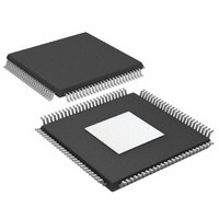
AD9779BSVZ Analog Devices Inc, AD9779BSVZ Datasheet - Page 27

AD9779BSVZ
Manufacturer Part Number
AD9779BSVZ
Description
IC DAC 16BIT DUAL 1GSPS 100TQFP
Manufacturer
Analog Devices Inc
Datasheet
1.AD9776BSVZRL.pdf
(56 pages)
Specifications of AD9779BSVZ
Data Interface
Serial
Number Of Bits
16
Number Of Converters
2
Voltage Supply Source
Analog and Digital
Power Dissipation (max)
300mW
Operating Temperature
-40°C ~ 85°C
Mounting Type
Surface Mount
Package / Case
100-TQFP Exposed Pad, 100-eTQFP, 100-HTQFP, 100-VQFP
Resolution (bits)
16bit
Sampling Rate
1GSPS
Input Channel Type
Parallel
Digital Ic Case Style
QFP
No. Of Pins
160
Operating Temperature Range
-40°C To +85°C
Lead Free Status / RoHS Status
Lead free / RoHS Compliant
For Use With
AD9779A-EBZ - BOARD EVALUATION FOR AD9779A
Settling Time
-
Lead Free Status / RoHS Status
Lead free / RoHS Compliant, Lead free / RoHS Compliant
Available stocks
Company
Part Number
Manufacturer
Quantity
Price
Company:
Part Number:
AD9779BSVZ
Manufacturer:
AD
Quantity:
2 100
Company:
Part Number:
AD9779BSVZ
Manufacturer:
ADI
Quantity:
325
Company:
Part Number:
AD9779BSVZ
Manufacturer:
Analog Devices Inc
Quantity:
10 000
Part Number:
AD9779BSVZ
Manufacturer:
ADI/亚德诺
Quantity:
20 000
Company:
Part Number:
AD9779BSVZRL
Manufacturer:
Analog Devices Inc
Quantity:
10 000
SPI REGISTER MAP
Table 11.
Register
Name
Comm
Digital
Control
Sync
Control
PLL
Control
Misc
Control
I DAC
Control
Register
Aux DAC1
Control
Register
Q DAC
Control
Register
Aux DAC2
Control
Register
Interrupt
Register
Address
0x00
0x01
0x02
0x03
0x04
0x05
0x06
0x07
0x08
0x09
0x0A
0x0B
0x0C
0x0D
0x0E
0x0F
0x10
0x11
0x12
0x13
to
0x18
0x19
0x1A
to
0x1F
00
01
02
03
04
05
06
07
08
09
10
11
12
13
14
15
16
17
18
19 to 24
25
26 to 31
Bit 7
SDIO
Bidirectional
Data Format
Sync
Receiver
Enable
PLL Enable
I DAC Sleep
Auxiliary
DAC1 Sign
Q DAC Sleep
Filter Interpolation Factor<1:0>
DAC2 Sign
PLL Control Voltage Range<2:0> (Read Only)
Auxiliary
Data Clock Delay Mode<1:0>
Bit 6
LSB/MSB First
Dual/Interleaved
Data Bus Mode
Sync Driver
Enable
PLL VCO Divider Ratio<1:0>
I DAC Power
Down
Current Direction
Current Direction
Auxiliary DAC1
Auxiliary DAC2
Sync Delay IRQ
Q DAC Power-
Data Clock Delay<3:0>
Sync Input Delay<3:0>
Sync Out Delay<3:0>
Down
PLL Band Select<5:0>
Rev. A | Page 27 of 56
Bit 5
Software
Reset
Real Mode
Sync
Triggering
Edge
Auxiliary
Auxiliary
Power-
Power-
Data Clock Divide
Down
DAC1
DAC2
Down
Q DAC Gain Adjustment<7:0>
Ratio<1:0>
I DAC Gain Adjustment<7:0>
Auxiliary DAC1 Data<7:0>
Auxiliary DAC2 Data<7:0>
Filter Modulation Mode<3:0>
Bit 4
Power-
Down
Mode
Data
Clock
Delay
Enable
Ratio<1:0>
Reserved
Reserved
PLL Loop
Divide
Bit 3
Auto
Power-
Down
Enable
Inverse
Sinc
Enable
Input Sync Pulse Frequency Ratio<2:0>
PLL Loop Bandwidth Adjustment<4:0>
Input Sync Pulse Timing Error Tolerance<3:0>
Output Sync Pulse Divide<2:0>
DAC Clock Offset<4:0>
Bit 2
DATACLK
Invert
AD9776/AD9778/AD9779
PLL Bias Setting<2:0>
Enable
Delay
Sync
IRQ
Reserved
Bit 1
PLL Lock
Indicator
(Read
Only)
TxEnable
Invert
Adjustment<9:8>
Adjustment<9:8>
Auxiliary DAC1
Auxiliary DAC2
PLL VCO AGC
Q DAC Gain
I DAC Gain
Data<9:8>
Data<9:8>
Gain<1:0>
Bit 0
Zero
Stuffing
Enable
Q First
Sync Out
Delay<4>
Sync Input
Delay<4>
Loopback
Internal
Sync
Def.
0x00
0x00
0x00
0x00
0x00
0x00
0x00
0x00
0xCF
0x37
0x38
0xF9
0x01
0x00
0x00
0xF9
0x01
0x00
0x00
0x00


