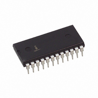
HI1-565AJD-5 Intersil, HI1-565AJD-5 Datasheet - Page 6

HI1-565AJD-5
Manufacturer Part Number
HI1-565AJD-5
Description
CONV D/A 12BIT 6.7MHZ 24-DIP
Manufacturer
Intersil
Datasheet
1.HI1-565AJD-5.pdf
(9 pages)
Specifications of HI1-565AJD-5
Number Of Bits
12
Data Interface
Parallel
Number Of Converters
1
Voltage Supply Source
Dual ±
Power Dissipation (max)
250mW
Operating Temperature
0°C ~ 75°C
Mounting Type
Through Hole
Package / Case
24-DIP (0.600", 15.24mm)
Lead Free Status / RoHS Status
Lead free / RoHS Compliant
Settling Time
-
Available stocks
Company
Part Number
Manufacturer
Quantity
Price
Settling Time
This is a challenging measurement, in which the result
depends on the method chosen, the precision and quality of
test equipment and the operating configuration of the DAC
(test conditions). As a result, the different techniques in use
by converter manufacturers can lead to consistently different
results. An engineer should understand the advantage and
limitations of a given test method before using the specified
settling time as a basis for design.
The previous approach calls for a strobed comparator to
sense final perturbations of the DAC output waveform. This
gives the LSB a reasonable magnitude (814µV for the
HI-565A), which provides the comparator with enough
overdrive to establish an accurate ±0.5 LSB window about the
final settled value. Also, the required test conditions simulate
the DACs environment for a common application - use in a
successive approximation A/D converter. Considerable
experience has shown this to be a reliable and repeatable
way to measure settling time.
The usual specification is based on a 10V step, produced by
simultaneously switching all bits from off-to-on (t
to-off (t
measured from 50% of the digital input transition to the final
entry within a window of ±0.5 LSB about the settled value.
Four measurements characterize a given type of DAC:
(a) t
(b) t
(c) t
(d) t
OFF
ON
ON
OFF
OFF
, to final value +0.5 LSB
, to final value -0.5 LSB
, to final value +0.5 LSB
, to final value -0.5 LSB
). The slower of the two cases is specified, as
100Ω
REF
R4
GND
6
IN
REF
REF OUT
6
5
19.95K
+
-
4
FIGURE 2. BIPOLAR VOLTAGE OUTPUT
V CC
10V
3
3.5K
ON
3K
) or on-
0.5mA
I REF
-V
HI-565A
EE
+
-
7
100Ω
PWR
GND
R3
12
MSB
24
INPUT
CODE
(4 x I REF
DAC
x CODE)
(Cases (b) and (c) may be eliminated unless the overshoot
exceeds 0.5 LSB). For example, refer to Figure 3 for the
measurement of case (d).
Procedure
As shown in Figure 3B, settling time equals t
comparator delay (t
13
9.95K
OFF.
• Adjust the delay on generator No. 2 for a t
• Switch on the LSB (+5V).
• Adjust the V
• Switch the LSB to Pulse (P).
• Readjust the V
• Adjust the V
• Reduce generator No. 2 delay until comparator output
• Measure t
LSB
BIP.
I O
microseconds. This assures that the DAC output has
settled to its final value.
COMPARATOR OUT. This is indicated by traces of
equal brightness on the oscilloscope display as shown
in Figure 3B. Note DVM reading.
and note DVM reading. One LSB equals one tenth the
difference in the DVM readings noted above.
5 LSBs (DVM reads 10X, so this sets the comparator to
sense the final settled value minus 0.5 LSB).
Comparator output disappears.
reappears, and adjust for “equal brightness”.
time equals t
2.5K
8
5K
5K
X
11
10
9
LSB
DAC
OUT
from scope as shown in Figure 3B. Settling
LSB
X
D
20V SPAN
10V SPAN
LSB
+ t
supply for 50% triggering at
= 15ns). To measure t
supply to reduce the DVM reading by
D
R (SEE
, i.e., t
+
supply for 50% triggering as before,
-
TABLE 2)
C
V O
X
+ 15ns.
X
X
:
plus the
X
of several


