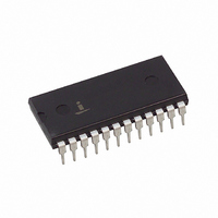
HI1-565AJD-5 Intersil, HI1-565AJD-5 Datasheet - Page 7

HI1-565AJD-5
Manufacturer Part Number
HI1-565AJD-5
Description
CONV D/A 12BIT 6.7MHZ 24-DIP
Manufacturer
Intersil
Datasheet
1.HI1-565AJD-5.pdf
(9 pages)
Specifications of HI1-565AJD-5
Number Of Bits
12
Data Interface
Parallel
Number Of Converters
1
Voltage Supply Source
Dual ±
Power Dissipation (max)
250mW
Operating Temperature
0°C ~ 75°C
Mounting Type
Through Hole
Package / Case
24-DIP (0.600", 15.24mm)
Lead Free Status / RoHS Status
Lead free / RoHS Compliant
Settling Time
-
Available stocks
Company
Part Number
Manufacturer
Quantity
Price
Other Considerations
Grounds
The Hl-565A has two ground terminals, pin 5 (REF GND)
and pin 12 (PWR GND). These should not be tied together
near the package unless that point is also the system signal
ground to which all returns are connected. (If such a point
exists, then separate paths are required to pins 5 and 12).
The current through pin 5 is near-zero DC (Note 1); but pin
12 carries up to 1.75mA of code-dependent current from bits
1, 2, and 3. The general rule is to connect pin 5 directly to
the system “quiet” point, usually called signal or analog
ground. Connect pin 12 to the local digital or power ground.
Then, of course, a single path must connect the
analog/signal and digital/power grounds.
Layout
Connections to pin 9 (I
for high speed performance. Output capacitance of the DAC
is only 20pF, so a small change or additional capacitance
may alter the op amp’s stability and affect settling time.
Connections to pin 9 should be short and few. Component
leads should be short on the side connecting to pin 9 (as for
feedback capacitor C). See the Settling Time section.
(A)
+5V
OUT
P
~100kHz
24
23
14
13
GENERATOR
LSB
PULSE
9.95K
NO. 1
2mA
HI-565A
12
5K
2.5K
TRIG
OUT
5K
OUT
SYNC
DVM
FIGURE 3A.
IN
) on the Hl-565A are most critical
8
11
10
9
5
NC
7
GENERATOR
20V ±20%
BIAS
PULSE
NO. 2
10
TURN ON
TURN OFF
(B)
SCHOTTKY
DIODES
90
OUT
200K
0.1µF
(C)
STROBE
IN (D)
COMP
OUT
SUPPLY
V
LSB
Bypass Capacitors
Power supply bypass capacitors on the op amp will serve
the HI-565A also. If no op amp is used, a 0.01µF ceramic
capacitor from each supply terminal to pin 12 is sufficient,
since supply current variations are small.
Current Cancellation
Current cancellation is a two step process within the
HI-565A in which code dependent variations are eliminated,
then the resulting DC current is supplied internally. First an
auxiliary 9-bit R-2R ladder is driven by the complement of
the DACs input code. Together, the main and auxiliary
ladders draw a continuous 2.25mA from the internal ground
node, regardless of input code. Part of this DC current is
supplied by the zener voltage reference, and the remainder
is sourced from the positive supply via a current mirror which
is laser trimmed for zero current through the external
terminal (pin 5).
(TURN
OFF)
(A)
(B)
(C)
(D)
-400mV
0.8V
+3V
0V
0V
2V
4V
0V
50%
50%
t
FIGURE 3B.
X
SETTLING TIME
t
D
-0.5 LSB
= COMPARATOR DELAY
EQUAL
BRIGHTNESS
DIGITAL
INPUT
DAC
OUTPUT
COMP.
STROBE
COMP.
OUT


