AD8349-EVAL Analog Devices Inc, AD8349-EVAL Datasheet
AD8349-EVAL
Specifications of AD8349-EVAL


AD8349-EVAL Summary of contents
Page 1
... BIAS ENOP 8 Figure 1. The AD8349 can be used as a direct-to-RF modulator in digital communication systems such as GSM, CDMA, and WCDMA base stations, and QPSK or QAM broadband wireless access transmitters. Its high dynamic range and high modulation accuracy also make it a perfect IF modulator in local multipoint distribution systems (LMDS) using complex modulation formats ...
Page 2
... AD8349 TABLE OF CONTENTS Specifications..................................................................................... 3 Absolute Maximum Ratings............................................................ 5 ESD Caution.................................................................................. 5 Pin Configuration and Functional Descriptions.......................... 6 Equivalent Circuits ........................................................................... 7 Typical Performance Characteristics ............................................. 8 Circuit Description......................................................................... 14 Overview...................................................................................... 14 LO Interface................................................................................. 14 V-to-I Converter......................................................................... 14 Mixers .......................................................................................... 14 D-to-S Amplifier......................................................................... 14 Bias Circuit .................................................................................. 14 Output Enable ............................................................................. 14 Basic Connections .......................................................................... 15 Baseband I and Q Inputs ........................................................... 15 Single-Ended Baseband Drive .................................................. 15 LO Input Drive Level ...
Page 3
... BB OUT = 4 MHz –4.5 dBm BB OUT = 2 dBm OUT + (3 × F )), P = 2.4 dBm LO BB OUT = 4 MHz –6.5 dBm BB OUT = –17.3 dBm CHAN Rev Page AD8349 Min Typ Max Unit 700 2700 MHz 1 dBm 7.6 dBm –45 –30 dBm –35 –31 dBc –39 –36 ...
Page 4
... AD8349 Parameter Conditions Bandwidth (3 dB 1500 MHz, baseband input = 600 mV p-p sine wave on 400 1500 MHz, baseband input = 60 mV p-p sine wave on 400 mV dc OUTPUT ENABLE Pin ENOP Off Isolation ENOP Low Turn-On Settling Time ENOP Low to High (90% of envelope) Turn-Off Settling Time ...
Page 5
... V, 2.5 V other conditions above those indicated in the operational 10 dBm section of this specification is not implied. Exposure to absolute 800 mW maximum rating conditions for extended periods may affect 30°C/W device reliability. 125°C −40°C to +85°C −65°C to +150°C Rev Page AD8349 ...
Page 6
... Positive Supply Voltage (4. 5.5 V) for the Baseband Input V-to-I Converters, Mixer Core, Band Gap Reference, and Output Amplifer. VPS1 and VPS2 should be connected to the same supply. To ensure adequate external bypassing, connect 0.1 µF and 100 pF capacitors between VPS2 and ground. IBBP QBBP 1 16 AD8349 IBBN QBBN 2 15 COM1 COM3 3 ...
Page 7
... EQUIVALENT CIRCUITS VPS2 IBBP COM3 Figure 3. Circuit A VPS1 LOIN LOIP COM1 Figure 4. Circuit B VPS2 ENOP COM3 Figure 5. Circuit C 40Ω 40Ω Figure 6. Circuit D Rev Page AD8349 VPS2 VOUT COM2 ...
Page 8
... AD8349 TYPICAL PERFORMANCE CHARACTERISTICS 5.25V 4.75V –1 –2 –3 –4 700 900 1100 1300 1500 1700 1900 2100 2300 2500 2700 LO FREQUENCY (MHz) Figure 7. Single Sideband (SSB) Output Power (P (I and Q Inputs Driven in Quadrature at Baseband Frequency (F I and Q Inputs at 1.2 V p-p Differential, T ...
Page 9
... LO FREQUENCY (MHz MHz, I and Q Inputs LO BB Driven in Quadrature at 1.2 V p-p Differential 4.75V V = 5.25V BASEBAND FREQUENCY (MHz 2140 MHz, I and Q Inputs BB LO Driven in Quadrature at 1.2 V p-p Differential 4.75V 5.25V S –40 –30 –20 – TEMPERATURE ( ° C) AD8349 = 25°C) A 100 = 25° 2140 MHz, LO ...
Page 10
... AD8349 –10 3USB, dBc –15 SSB, dBm –20 –25 –30 –35 USB, dBC –40 –45 –50 LO, dBm –55 –60 –65 –70 0.2 0.4 0.6 0.8 1.0 1.2 1.4 1.6 1.8 2.0 BASEBAND DIFFERENTIAL INPUT VOLTAGE (V p-p) Figure 19. Third Order Distortion (3USB), Carrier Feedthrough, Sideband Suppression, and SSB P vs ...
Page 11
... MHz Figure 30. 20 MHz Offset Noise Floor Distribution 25° MHz, I and Q Inputs Driven in Quadrature at 1 Rev Page AD8349 NOISE FLOOR (dBm/Hz) = 940 MHz LO = 25°C) A NOISE FLOOR (dBm/Hz) = 1960 MHz LO = 25°C) A NOISE FLOOR (dBm/Hz) = 2140 MHz LO = 25°C) ...
Page 12
... AD8349 –140 –142 –144 –146 –148 WITH AC INPUT –150 –152 –154 WITHOUT AC INPUT –156 –158 –160 –10 –8 –6 –4 –2 LO INPUT (dBm) Figure 31. 20 MHz Offset Noise Floor vs. LO Input Power (F = 2140 MHz 25° –10 –15 –20 –25 – 1900MHz LO – ...
Page 13
... A I and Q Inputs at a bias of 400 mV +85° –40° –45 –75 –70 –65 –60 –55 –50 SIDEBAND SUPPRESSION (dBc) AFTER NULLING TO < –50dBc AT +25°C = 25° MHz, I and Q Inputs biased at 0 AD8349 –50 –45 = 2140 MHz, LO –40 –35 = 2140 MHz, LO ...
Page 14
... AD8349 CIRCUIT DESCRIPTION OVERVIEW The AD8349 can be divided into five sections: the local oscil- lator (LO) interface, the baseband voltage-to-current (V-to-I) converter, the mixers, the differential-to-single-ended (D-to-S) amplifier, and the bias circuit. A detailed block diagram of the device is shown in Figure 42. LOIP PHASE SPLITTER ...
Page 15
... WCDMA and GSM/EDGE systems. Reducing the baseband drive level also has the benefit of increasing the bandwidth of the baseband input. This would allow the AD8349 to be used in applications requiring a high modulation bandwidth, e.g., as the IF modulator in high data- rate microwave radios. SINGLE-ENDED BASEBAND DRIVE ...
Page 16
... LO input port. Because the LO input pins are internally dc-biased, ac coupling capacitors must be used on each LO input pin. Rev Page 100pF 0.1µF 100pF VPS1 VPS2 IBBP IBBN VOUT Σ LOIP PHASE QBBP SPLITTER LOIN QBBN AD8349 COM1 COM2 COM3 0.1µF ...
Page 17
... Figure 24 result, no additional matching circuitry is required if the output is driving a 50 Ω load. The –45 output power of the AD8349 under nominal conditions –46 (1.2 V p-p differential baseband drive, 400 mV dc baseband bias, and supply) is shown in Figure 7. –47 OUTPUT ENABLE – ...
Page 18
... DACs in a single package. AD9777 INTERFACE The AD977x family of dual DACs is well suited to driving the baseband inputs of the AD8349. The AD9777 is a dual 16-bit DAC that can generate either a baseband output or a complex IF using the device’s complex modulator. The basic interface between the AD9777’s I AD8349’ ...
Page 19
... Figure 53. AD8349 Single Sideband Spectrum at 2140 MHz REDUCING UNDESIRED SIDEBAND LEAKAGE Undesired sideband leakage is the result of phase and amplitude imbalances between the I and Q channel baseband signals. Therefore, to reduce the undesired sideband leakage, the amplitude and phase of the baseband signals have to be matched at the mixer cores ...
Page 20
... Figure 55. AD8349 Single Sideband Spectrum at 2140 MHz after LO Nulling SIDEBAND SUPPRESSION AND LO FEEDTHROUGH VS. TEMPERATURE In practical applications, reduction of LO feedthrough and undesired sideband suppression can be performed as a one time calibration, with the required correction factors being stored in nonvolatile RAM ...
Page 21
... Figure 59. Single-Carrier WCDMA ACPR and Noise Floor (dBm/Hz MHz WCDMA MULTICARRIER APPLICATION The high dynamic range of the AD8349 also permits use in multicarrier WCDMA applications. Figure 60 shows a 4-carrier WCDMA spectrum at 1960 MHz per-carrier power of –24.2 dBm, an ACPR of –60.4dB is achieved. Figure 61 shows the variation in ACP and noise floor (dBc/Hz) with output power ...
Page 22
... AD8349 –54 –55 –56 –57 2140 ADJ CPR –58 1960 ADJ CPR –59 –60 –61 –62 2140 ALT CPR –63 –64 1960 NOISE –65 2140 NOISE –66 –29 –28 –27 –26 –25 –24 –23 –22 –21 –20 –19 –18 –17 CHANNEL POWER (dBm) Figure 61 ...
Page 23
... The user should be aware that while the use of the integrated synthesizer might come at the expense of slightly degraded noise performance from the AD8349, it can be a much cheaper alternative to a separate PLL and VCO solution. Figure 61 shows the options available. Table 5. ADF4360 Family Operating Frequencies ...
Page 24
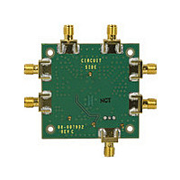
... Baseband Input Filters: These components can be used to implement a low-pass filter for the C8–C11 baseband signals. designed without any components on the underside of the board so that heat may be applied under the AD8349 for easy removal and replacement of the DUT. Figure 67. Evaluation Board Silkscreen via pull-up resistor R10. ...
Page 25
... C10 OPEN 3 COM1 COM3 14 TP1 GND COM1 COM3 LOIN VPS2 12 C5 100pF LOIP VOUT 6 11 VPS1 COM3 100pF 8 ENOP COM2 9 TP2 ENOP 49.9Ω Figure 68. Evaluation Board Schematic Rev Page AD8349 QP QN TP3 VPOS R11 +V S 0Ω C6 0.1µF VOUT ...
Page 26
... AD8349 CHARACTERIZATION SETUPS SSB SETUP The primary setup used to characterize the AD8349 is shown in Figure 69. This setup was used to evaluate the product as a single-sideband modulator. The interface board has circuitry that converts the single-ended I and Q inputs from the arbitrary function generator to differential inputs with a dc bias of 400 mV ...
Page 27
... OUTLINE DIMENSIONS Figure 70. 16-Lead Thin Shrink Small Outline with Exposed Pad [TSSOP/EP] ORDERING GUIDE Model Temperature Range (°C) AD8349ARE –40 to +85 AD8349ARE-REEL7 –40 to +85 1 AD8349AREZ –40 to +85 AD8349AREZ-REEL7 1 –40 to +85 AD8349-EVAL Pb-free part. 5.10 5.00 4. 4.50 TOP 6.40 4.40 VIEW BSC 4.30 ...
Page 28
... AD8349 NOTES © 2004 Analog Devices, Inc. All rights reserved. Trademarks and registered trademarks are the property of their respective owners. C03570-0-11/04(A) Rev Page ...