AD8349-EVAL Analog Devices Inc, AD8349-EVAL Datasheet - Page 2
AD8349-EVAL
Manufacturer Part Number
AD8349-EVAL
Description
Manufacturer
Analog Devices Inc
Datasheet
1.AD8349-EVAL.pdf
(28 pages)
Specifications of AD8349-EVAL
Lead Free Status / Rohs Status
Not Compliant


AD8349
TABLE OF CONTENTS
Specifications..................................................................................... 3
Absolute Maximum Ratings............................................................ 5
Pin Configuration and Functional Descriptions.......................... 6
Equivalent Circuits ........................................................................... 7
Typical Performance Characteristics ............................................. 8
Circuit Description......................................................................... 14
Basic Connections .......................................................................... 15
REVISION HISTORY
11/04—Data Sheet Changed from Rev. 0 to Rev. A
Changes to Figure 25 through Figure 30 ................................11
Changes to Figure 37 through Figure 39 ................................13
Change to WCDMA MultiCarrier Application section .......21
Change to Figure 60 and Figure 61 .........................................21
11/03—Revision 0: Initial Version
ESD Caution.................................................................................. 5
Overview...................................................................................... 14
LO Interface................................................................................. 14
V-to-I Converter......................................................................... 14
Mixers .......................................................................................... 14
D-to-S Amplifier......................................................................... 14
Bias Circuit .................................................................................. 14
Output Enable ............................................................................. 14
Baseband I and Q Inputs ........................................................... 15
Single-Ended Baseband Drive .................................................. 15
LO Input Drive Level ................................................................. 16
Frequency Range ........................................................................ 16
LO Input Impedance Matching ................................................ 16
Single-Ended LO Drive.............................................................. 17
Rev. A | Page 2 of 28
Applications..................................................................................... 21
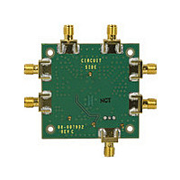
Evaluation Board ............................................................................ 24
Characterization Setups................................................................. 26
Outline Dimensions ....................................................................... 27
RF Output.................................................................................... 17
Output Enable............................................................................. 17
Baseband DAC Interface ........................................................... 18
AD9777 Interface ....................................................................... 18
Biasing and Filtering .................................................................. 18
Reducing Undesired Sideband Leakage .................................. 19
Reduction of LO Feedthrough ................................................. 19
Sideband Suppression and LO Feedthrough vs. Temperature
....................................................................................................... 20
3GPP WCDMA Single-Carrier Application ........................... 21
WCDMA MultiCarrier Application ........................................ 21
GSM/EDGE Application ........................................................... 22
Soldering Information ............................................................... 23
LO Generation Using PLLs ....................................................... 23
Transmit DAC Options ............................................................. 23
SSB Setup..................................................................................... 26
Ordering Guide .......................................................................... 27