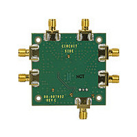
AD8349-EVAL Analog Devices Inc, AD8349-EVAL Datasheet - Page 14
AD8349-EVAL
Manufacturer Part Number
AD8349-EVAL
Description
Manufacturer
Analog Devices Inc
Datasheet
1.AD8349-EVAL.pdf
(28 pages)
Specifications of AD8349-EVAL
Lead Free Status / Rohs Status
Not Compliant


AD8349
CIRCUIT DESCRIPTION
OVERVIEW
The AD8349 can be divided into five sections: the local oscil-
lator (LO) interface, the baseband voltage-to-current (V-to-I)
converter, the mixers, the differential-to-single-ended (D-to-S)
amplifier, and the bias circuit. A detailed block diagram of the
device is shown in Figure 42.
The LO interface generates two LO signals at 90 degrees of
phase difference to drive two mixers in quadrature. Baseband
signals are converted into currents by the V-to-I converters,
which feed into the two mixers. The outputs of the mixers
combine to feed the differential-to-single-ended amplifier,
which provides a 50 Ω output interface. Reference currents to
each section are generated by the bias circuit. Additionally, the
RF output is controlled by an output enable pin (ENOP), which
is capable of switching the output on and off within 50 ns. A
detailed description of each section follows.
LO INTERFACE
The LO interface consists of interleaved stages of buffer
amplifiers and polyphase phase splitters. An input buffer
provides a 50 Ω termination to the LO signal source driving
LOIP and LOIN. The buffer also increases the LO signal
amplitude to drive the phase splitter. The phase splitter is
formed by an R-C polyphase network that splits the buffered
LO signal into two parts in precise quadrature phase relation
with each other. Each LO signal then passes through a buffer
amplifier to compensate for the signal loss through the phase
splitter. The two signals pass through another polyphase
network to enhance the quadrature accuracy over the full
operating frequency range. The outputs of the second phase
splitter are fed into the driver amplifiers for the mixers’ LO
inputs.
QBBP
QBBN
LOIN
IBBP
IBBN
LOIP
Figure 42. Block Diagram
SPLITTER
PHASE
Σ
OUT
Rev. A | Page 14 of 28
V-TO-I CONVERTER
The differential baseband input voltages that are applied to the
baseband input pins are fed to two op amps that perform a
differential voltage-to-current conversion. The differential
output currents of these op amps then feed each of their
respective mixers.
MIXERS
The AD8349 has two double-balanced mixers, one for the in-
phase channel (I channel) and one for the quadrature channel
(Q channel). Both mixers are based on the Gilbert cell design of
four cross-connected transistors. The output currents from the
two mixers sum together in a pair of resistor-inductor (R-L)
loads. The signals developed across the R-L loads are sent to the
D-to-S amplifier.
D-TO-S AMPLIFIER
The output D-to-S amplifier consists of two emitter followers
driving a totem pole output stage. Output impedance is estab-
lished by the emitter resistors in the output transistors. The
output of this stage connects to the output (VOUT) pin.
BIAS CIRCUIT
A band gap reference circuit generates the proportional-to-
absolute-temperature (PTAT) reference currents used by
different sections. The band gap reference circuit also generates
a temperature stable current in the V-to-I converters to produce
a temperature independent slew rate.
OUTPUT ENABLE
During normal operation (ENOP = high), the output current
from the V-to-I converters feeds into the mixers, where they
mix with the two phases of LO signals. When ENOP is pulled
low, the V-to-I output currents are steered away from the
mixers, thus turning off the RF output. Power to the final stage
of LO drivers is also removed to minimize LO feedthrough.
Even when the output is disabled, the differential-to-single-
ended stage is still powered up to maintain constant output
impedance.