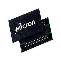
MT46V64M8FN-6:F Micron Technology Inc, MT46V64M8FN-6:F Datasheet - Page 75

MT46V64M8FN-6:F
Manufacturer Part Number
MT46V64M8FN-6:F
Description
DRAM Chip DDR SDRAM 512M-Bit 64Mx8 2.5V 60-Pin FBGA Tray
Manufacturer
Micron Technology Inc
Type
DDR SDRAMr
Datasheet
1.MT46V32M16P-5BF_TR.pdf
(91 pages)
Specifications of MT46V64M8FN-6:F
Package
60FBGA
Density
512 Mb
Address Bus Width
15 Bit
Operating Supply Voltage
2.5 V
Maximum Clock Rate
333 MHz
Maximum Random Access Time
0.7 ns
Operating Temperature
0 to 70 °C
Organization
64Mx8
Address Bus
15b
Access Time (max)
700ps
Operating Supply Voltage (typ)
2.5V
Package Type
FBGA
Operating Temp Range
0C to 70C
Operating Supply Voltage (max)
2.7V
Operating Supply Voltage (min)
2.3V
Supply Current
175mA
Pin Count
60
Mounting
Surface Mount
Operating Temperature Classification
Commercial
Lead Free Status / Rohs Status
Not Compliant
Available stocks
Company
Part Number
Manufacturer
Quantity
Price
Company:
Part Number:
MT46V64M8FN-6:F TR
Manufacturer:
Micron Technology Inc
Quantity:
10 000
Figure 39:
PDF: 09005aef80a1d9d4/Source: 09005aef82a95a3a
DDR_x4x8x16_Core2.fm - 512Mb DDR: Rev. N; Core DDR Rev. B 2/09 EN
t DQSS (NOM)
Command
Consecutive WRITE-to-WRITE
Address
DQS
CK#
DM
Notes:
DQ
CK
WRITE
Bank,
1. DI b (or n) = data-in from column b (or column n).
2. Three subsequent elements of data-in are applied in the programmed order following DI b.
3. Three subsequent elements of data-in are applied in the programmed order following DI n.
4. An uninterrupted burst of 4 is shown.
5. Each WRITE command may be to any bank.
Col b
T0
t DQSS
NOP
DI
T1
b
T1n
WRITE
Bank,
Col n
T2
75
T2n
Micron Technology, Inc., reserves the right to change products or specifications without notice.
NOP
T3
DI
n
T3n
Transitioning Data
512Mb: x4, x8, x16 DDR SDRAM
NOP
T4
T4n
©2000 Micron Technology, Inc. All rights reserved.
T5
NOP
Don’t Care
Operations


