AD7394AR Analog Devices Inc, AD7394AR Datasheet
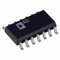
IC DAC 12BIT SRL 3V 14-SOIC

AD7394AR

Manufacturer Part Number
AD7394AR
Description
IC DAC 12BIT SRL 3V 14-SOIC
Manufacturer
Analog Devices Inc
Datasheet

Specifications of AD7394AR

Rohs Status
RoHS non-compliant
Settling Time
60µs
Number Of Bits
12
Data Interface
Serial
Number Of Converters
2
Voltage Supply Source
Single Supply
Power Dissipation (max)
1mW
Operating Temperature
-40°C ~ 85°C
Mounting Type
Surface Mount
Package / Case
14-SOIC (3.9mm Width), 14-SOL

Available stocks

Company
Part Number
Manufacturer
Quantity
Price
Part Number:
AD7394AR
Manufacturer:
ADI/亚德诺
Quantity:
20 000
Part Number:
AD7394ARZ
Manufacturer:
PANASONIC
Quantity:
560
Part Number:
AD7394ARZ
Manufacturer:
ADI/亚德诺
Quantity:
20 000
Part Number:
AD7394ARZ-REEL7
Manufacturer:
ADI/亚德诺
Quantity:
20 000
a
GENERAL DESCRIPTION
The AD7394/AD7395 family of dual, 12-/10-bit, voltage output
digital-to-analog converters is designed to operate from a single
+3 V supply. Built using a CBCMOS process, this monolithic
DAC offers the user low cost and ease of use in single-supply
+3 V systems. Operation is guaranteed over the supply voltage
range of +2.7 V to +5.5 V making this device ideal for battery
operated applications.
The full-scale output voltage is determined by the applied exter-
nal reference input voltage, VREF. The rail-to-rail VREF input
to V
positive supply V
A doubled-buffered serial data interface offers high speed,
microcontroller compatible inputs using serial-data-in (SDI),
clock (CLK) and load strobe (LDA + LDB) pins. A chip-select
(CS) pin simplifies connection of multiple DAC packages by
enabling the clock input when active low. Additionally, an RS
input sets the output to zero scale or to 1/2 scale based on the
logic level applied to the MSB pin. The power shutdown pin,
SHDN, reduces power dissipation to nanoamp current levels.
All digital inputs contain Schmitt-triggered logic levels to mini-
mize power dissipation and prevent false triggering on the clock
input.
Both parts are offered in the same pinout to allow users to select
the amount of resolution appropriate for their application with-
out circuit card redesign.
REV. 0
Information furnished by Analog Devices is believed to be accurate and
reliable. However, no responsibility is assumed by Analog Devices for its
use, nor for any infringements of patents or other rights of third parties
which may result from its use. No license is granted by implication or
otherwise under any patent or patent rights of Analog Devices.
FEATURES
Micropower: 100 A/DAC
0.1 A Typical Power Shutdown
Single-Supply +2.7 V to +5.5 V Operation
Compact 1.1 mm Height TSSOP-14 Package
AD7394/12-Bit Resolution
AD7395/10-Bit Resolution
Serial Interface with Schmitt Trigger Inputs
APPLICATIONS
Automotive Output Span Voltage
Portable Communications
Digitally Controlled Calibration
PC Peripherals
OUT
outputs allows for a full-scale voltage set equal to the
DD
or any value in between.
The AD7394/AD7395 is specified over the extended industrial
(–40 C to +85 C) temperature range. Packages available in-
clude plastic DIP and low profile 1.75 mm height SO-14 surface
mount packages. The AD7395ARU is available for ultracompact
applications in a thin 1.1 mm TSSOP-14 package. For automotive
applications the AD7395AR is specified for operation over the
(–40 C to +125 C) temperature range.
One Technology Way, P.O. Box 9106, Norwood, MA 02062-9106, U.S.A.
Tel: 781/329-4700
Fax: 781/326-8703
(DATA)
CLK
LDA
LDB
SDI
CS
Figure 1. Differential Nonlinearity Error vs. Code
–0.2
–0.4
–0.6
–0.8
0.8
0.6
0.4
0.2
–1
1
0
EN
0
T
SUPERIMPOSED
FUNCTIONAL BLOCK DIAGRAM
S
H
F
T
A
I
DGND
V
V
= –55 C, +25 C, +85 C
500
R
E
G
S
E
R
T
DD
REF
I
+3 V, Dual, Serial Input
= 3V
= 2.5V
World Wide Web Site: http://www.analog.com
1000
12
D
D
MSB
D
A
C
A
P R
D
A
C
B
P R
1500
AD7394/AD7395
R
E
G
S
E
R
R
E
G
S
E
R
T
T
I
I
CODE – Decimal
V
DD
12-/10-Bit DACs
2000
RS
V
REF
AD7394/AD7395
2500
© Analog Devices, Inc., 1998
DAC A
DAC B
3000
AGND
3500
OP
AMP A
OP
AMP B
SHDN
4000
V
V
OUTA
OUTB

Related parts for AD7394AR

AD7394AR Summary of contents

Page 1

FEATURES Micropower: 100 A/DAC 0.1 A Typical Power Shutdown Single-Supply +2 +5.5 V Operation Compact 1.1 mm Height TSSOP-14 Package AD7394/12-Bit Resolution AD7395/10-Bit Resolution Serial Interface with Schmitt Trigger Inputs APPLICATIONS Automotive Output Span Voltage Portable Communications ...

Page 2

AD7394/AD7395–SPECIFICATIONS AD7394 12-BIT RAIL-TO-RAIL VOLTAGE OUT DAC ELECTRICAL CHARACTERISTICS Parameter STATIC PERFORMANCE 1 Resolution 2 Relative Accuracy 2 Relative Accuracy 2 Differential Nonlinearity 2 Differential Nonlinearity Zero-Scale Error Full-Scale Voltage Error Full-Scale Voltage Error 3 Full-Scale Tempco REFERENCE INPUT V ...

Page 3

AD7395 10-BIT RAIL-TO-RAIL VOLTAGE OUT DAC ELECTRICAL CHARACTERISTICS Parameter STATIC PERFORMANCE 1 Resolution 2 Relative Accuracy 2 Relative Accuracy 2 Differential Nonlinearity Zero-Scale Error Full-Scale Voltage Error Full-Scale Voltage Error 3 Full-Scale Tempco REFERENCE INPUT V Range REF IN Input ...

Page 4

AD7394/AD7395 SDI CLK CS LDA,B SDI CLK LDA OUT ZS SHDN CS CLK RS SHDN MSB ...

Page 5

... Thin Shrink Surface Mount (RU-14 180 C/W Maximum Junction Temperature (T max 150 C J Res Temperature Model (LSB) Range AD7394AN 12 – +85 C AD7394AR 12 – +85 C AD7395AN 10 – +125 C AD7395AR 10 – +125 C AD7395ARU 10 – +85 C The AD7394/AD7395 contains 709 transistors. The die size measures 70 mil CAUTION ESD (electrostatic discharge) sensitive device ...

Page 6

AD7394/AD7395 Pin No. Name Function 1 AGND Analog Ground DAC A Voltage Output. OUTA 3 V DAC Reference voltage input terminal. Establishes DAC full-scale output voltage. Pin can be tied to V REF 4 DGND Digital Ground. Should ...

Page 7

– 2.5V REF A 1 0.5 0 –0 + –1 –1.5 0 500 1000 1500 2000 2500 3000 3500 4000 CODE – Decimal Figure ...

Page 8

AD7394/AD7395 1800 AD7394 1600 2.7V, CODE = 555 DD H 1400 2.7V, CODE = 3FF 5.5V, CODE = 155 DD H 1200 5.5V, CODE = 3FF ...

Page 9

OPERATION The AD7394 and AD7395 are a set of pin compatible, dual, 12-bit/10-bit digital-to-analog converters. These single-supply operation devices consume less than 200 microamps of current while operating from power supplies in the +2 +5.5 V range, making ...

Page 10

AD7394/AD7395 POWER SUPPLY The very low power consumption of the AD7394/AD7395 is a direct result of a circuit design optimizing the use of a CBCMOS process. By using the low power characteristics of CMOS for the logic, and the low ...

Page 11

MSB BYTE 1 B15 B14 B13 B12 B11 D11 D11–D0: 12-bit AD7394 DAC data; D9–D0: 10-bit AD7395 DAC data Don’t Care; The MSB of byte 1 is the first ...

Page 12

AD7394/AD7395 output drive current, but consumes only 50 microamps inter- nally. If higher resolution is required, the AD7394 can be used with the addition of two more bits of data inserted into the software coding, which would result in a ...

Related keywords