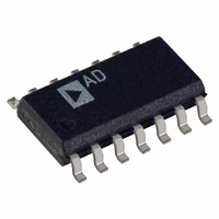
AD7394AR Analog Devices Inc, AD7394AR Datasheet - Page 9

AD7394AR
Manufacturer Part Number
AD7394AR
Description
IC DAC 12BIT SRL 3V 14-SOIC
Manufacturer
Analog Devices Inc
Datasheet
1.AD7394ARZ-REEL7.pdf
(12 pages)
Specifications of AD7394AR
Rohs Status
RoHS non-compliant
Settling Time
60µs
Number Of Bits
12
Data Interface
Serial
Number Of Converters
2
Voltage Supply Source
Single Supply
Power Dissipation (max)
1mW
Operating Temperature
-40°C ~ 85°C
Mounting Type
Surface Mount
Package / Case
14-SOIC (3.9mm Width), 14-SOL
Available stocks
Company
Part Number
Manufacturer
Quantity
Price
Part Number:
AD7394AR
Manufacturer:
ADI/亚德诺
Quantity:
20 000
Company:
Part Number:
AD7394ARZ
Manufacturer:
PANASONIC
Quantity:
560
Part Number:
AD7394ARZ
Manufacturer:
ADI/亚德诺
Quantity:
20 000
Part Number:
AD7394ARZ-REEL7
Manufacturer:
ADI/亚德诺
Quantity:
20 000
REV. 0
OPERATION
The AD7394 and AD7395 are a set of pin compatible, dual,
12-bit/10-bit digital-to-analog converters. These single-supply
operation devices consume less than 200 microamps of current
while operating from power supplies in the +2.7 V to +5.5 V
range, making them ideal for battery operated applications.
They contain a voltage-switched, 12-bit/10-bit, laser trimmed
digital-to-analog converter, rail-to-rail output op amps, two
DAC registers and a serial input shift register. The external
reference input has constant input resistance independent of the
digital code setting of the DAC. In addition, the reference input
can be tied to the same supply voltage as V
maximum output voltage span of 0 to V
consists of a serial data input (SDI), clock (CLK) and chip
select pin (CS) and two load DAC Register pins (LDA and
LDB). A reset (RS) pin is available to reset the DAC register to
zero scale or midscale, depending on the digital level applied to
the MSB pin. This function is useful for power-on reset or
system failure recovery to a known state. Additional power
savings are accomplished by activating the SHDN pin resulting
in a 1.5 A maximum consumption sleep mode.
D/A CONVERTER SECTION
The voltage switched R-2R DAC generates an output voltage
dependent on the external reference voltage connected to the
REF pin according to the following equation:
where D is the decimal data word loaded into the DAC register
and N is the number of bits of DAC resolution. In the case of
the 10-bit AD7395 using a 2.5 V reference, Equation 1 simpli-
fies to:
Using Equation 2 the nominal midscale voltage at V
1.25 V for D = 512; full-scale voltage is 2.497 V. The LSB step
size is = 2.5
For the 12-bit AD7394 operating from a 5.0 V reference Equa-
tion 1 becomes:
Using Equation 3 the AD7394 provides a nominal midscale
voltage of 2.50 V for D = 2048, and a full-scale output of
4.998 V. The LSB step size is = 5.0 1/4096 = 0.0012 V.
V
V
V
OUT
OUT
OUT
V
2.5 D
5.0 D
1024
4096
1/1024 = 0.0024 V.
REF
2
N
D
DD
. The serial interface
DD
, resulting in a
OUT
is
(1)
(2)
(3)
–9–
AMPLIFIER SECTION
The internal DAC’s output is buffered by a low power con-
sumption precision amplifier. The op amp has a 60 s typical
settling time to 0.1% of full scale. There are slight differences in
settling time for negative slewing signals versus positive. Also,
negative transition settling time to within the last 6 LSBs of zero
volts has an extended settling time. The rail-to-rail output stage
of this amplifier has been designed to provide precision perfor-
mance while operating near either power supply. Figure 20
shows an equivalent output schematic of the rail-to-rail-ampli-
fier with its N-channel pull-down FETs that will pull an output
load directly to GND. The output sourcing current is provided
by a P-channel pull-up device that can source current to GND
terminated loads.
The rail-to-rail output stage provides more than 1 mA of out-
put current. The N-channel output pull-down MOSFET shown
in Figure 20 has a 35
rent capability near ground. In addition to resistive load driving
capability, the amplifier has also been carefully designed and
characterized for up to 100 pF capacitive load driving capability.
REFERENCE INPUT
The reference input terminal has a constant input resistance
independent of digital code which results in reduced glitches on
the external reference voltage source. The high 2.5 M input
resistance minimizes power dissipation within the AD7394/
AD7395 D/A converters. The V
ranging from ground to the positive supply voltage V
the simplest applications, which saves an external reference
voltage source, is connection of the V
V
output span maximizing the programmed range. The reference
input will accept ac signals as long as they are kept within the
supply voltage range, 0 < V
and integral nonlinearity error performance are plotted in the
Typical Performance Characteristics section (see Figures 8 and
18). The ratiometric reference feature makes the AD7394/AD7395
an ideal companion to ratiometric analog-to-digital converters
such as the AD7896.
DD
supply. This connection results in a rail-to-rail voltage
Figure 20. Equivalent Analog Output Circuit
ON resistance, which sets the sink cur-
REF
< V
REF
AD7394/AD7395
DD
input accepts input voltages
REF
. The reference bandwidth
P-CH
N-CH
terminal to the positive
DD
V
V
AGND
. One of
DD
OUT


