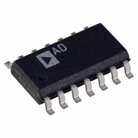
AD7394AR Analog Devices Inc, AD7394AR Datasheet - Page 6

AD7394AR
Manufacturer Part Number
AD7394AR
Description
IC DAC 12BIT SRL 3V 14-SOIC
Manufacturer
Analog Devices Inc
Datasheet
1.AD7394ARZ-REEL7.pdf
(12 pages)
Specifications of AD7394AR
Rohs Status
RoHS non-compliant
Settling Time
60µs
Number Of Bits
12
Data Interface
Serial
Number Of Converters
2
Voltage Supply Source
Single Supply
Power Dissipation (max)
1mW
Operating Temperature
-40°C ~ 85°C
Mounting Type
Surface Mount
Package / Case
14-SOIC (3.9mm Width), 14-SOL
Available stocks
Company
Part Number
Manufacturer
Quantity
Price
Part Number:
AD7394AR
Manufacturer:
ADI/亚德诺
Quantity:
20 000
Company:
Part Number:
AD7394ARZ
Manufacturer:
PANASONIC
Quantity:
560
Part Number:
AD7394ARZ
Manufacturer:
ADI/亚德诺
Quantity:
20 000
Part Number:
AD7394ARZ-REEL7
Manufacturer:
ADI/亚德诺
Quantity:
20 000
AD7394/AD7395
Pin
No.
1
2
3
4
5
6
7
8
9
10
11
12
13
14
Name
AGND
V
V
DGND
CS
CLK
SDI
LDA
RS
LDB
MSB
SHDN
V
V
OUTA
REF
DD
OUTB
Function
Analog Ground.
DAC A Voltage Output.
DAC Reference voltage input terminal. Establishes DAC full-scale output voltage. Pin can be tied to V
Digital Ground. Should be tied to analog GND.
Chip Select, active low input. Disables shift register loading when high. Does not effect LDA or LDB operation.
Clock input, positive edge clocks data into shift register, MSB data bit first.
Serial Data Input, input data loads directly into the shift register.
Load DAC register strobe, level sensitive active low. Transfers shift register data to DAC A register. Asyn-
chronous active low input. See Control Logic Truth Table for operation.
Resets DAC register to zero condition or half-scale, depending on MSB pin logic level. Asynchronous active
low input.
Load DAC register strobe, level-sensitive active low. Transfers shift register data to DAC B register. Asyn-
chronous active low input. See Control Logic Truth Table for operation.
Digital Input: Logic High presets DAC registers to half-scale 800
strobed; Logic Low clears all DAC registers to zero (000
Active low shutdown control input. Does not affect register contents as long as power is present on V
data can be loaded into the shift register and DAC register during shutdown. When device is powered up the
most recent data loaded into the DAC register will control the DAC output.
Positive power supply input. Specified range of operation +2.7 V to +5.5 V
DAC B Voltage Output.
PIN FUNCTION DESCRIPTIONS
V
PIN CONFIGURATIONS
AGND
DGND
OUTA
V
CLK
REF
SDI
CS
1
2
3
4
5
6
7
(Not to Scale)
TOP VIEW
AD7394
AD7395
–6–
14
13
12
11
10
9
8
V
V
SHDN
MSB
LDB
RS
LDA
OUTB
DD
H
) when the RS pin is strobed.
H
(sets MSB bit to one) when the RS pin is
DD
DD
. New
pin.
REV. 0


