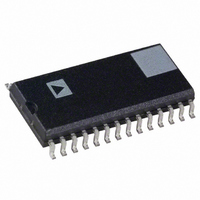
ADMCF341BR Analog Devices Inc, ADMCF341BR Datasheet - Page 11

ADMCF341BR
Manufacturer Part Number
ADMCF341BR
Description
IC DSP 3CH 12BIT MOT-CTRL 28SOIC
Manufacturer
Analog Devices Inc
Series
Motor Controlr
Type
Motor Controlr
Datasheet
1.ADMCF341BR.pdf
(36 pages)
Specifications of ADMCF341BR
Rohs Status
RoHS non-compliant
Interface
Synchronous Serial Port (SSP)
Clock Rate
20MHz
Non-volatile Memory
FLASH (12 kB), ROM (12kB)
On-chip Ram
2.5kB
Voltage - I/o
5.00V
Voltage - Core
5.00V
Operating Temperature
-40°C ~ 85°C
Mounting Type
Surface Mount
Package / Case
28-SOIC (7.5mm Width)
Available stocks
Company
Part Number
Manufacturer
Quantity
Price
Part Number:
ADMCF341BRZ
Manufacturer:
ADI/亚德诺
Quantity:
20 000
DSP Control Registers
The DSP core has a system control register, SYSCNTL,
memory-mapped at DM (0x3FFF). SPORT1 must be configured
as a serial port by setting Bit 10. SPORT0 and SPORT1 are
enabled by setting Bit 11 and Bit 12.
The DSP core has a wait state control register, MEMWAIT,
memory-mapped at DM (0x3FFE). The default value of this
register is 0xFFFF. For proper operation of the ADMC(F)341,
this register must always contain the value 0x8000. This value
sets the minimum access time to the program memory.
The configurations of both the SYSCNTL and MEMWAIT
registers of the ADMC(F)341 are shown in Figure 31.
THREE-PHASE PWM CONTROLLER
Overview
The PWM generator block of the ADMC(F)341 is a flexible,
programmable, three-phase PWM waveform generator that can
be programmed to generate the required switching patterns to
drive a three-phase voltage source inverter for ac induction
motors (ACIM) or permanent magnet synchronous motors
(PMSM). In addition, the PWM block contains special functions
that considerably simplify the generation of the required PWM
switching patterns for control of brushless dc motors (BDCM),
including electronically commutated motors (ECM).
The six PWM output signals consist of three high-side drive
signals (AH, BH, and CH) and three low-side drive signals
(AL, BL, and CL). The switching frequency, dead time, and
minimum pulse widths of the generated PWM patterns are
programmable using, respectively, the PWMTM, PWMDT, and
PWMPD registers. In addition, three registers (PWMCHA,
REV. B
PWM CONFIGURATION
PWMTM (15...0)
PWMDT (9...0)
PWMPD (9...0)
PWMSYNCWT (7...0)
MODECTRL (6)
TO INTERRUPT
CONTROLLER
REGISTERS
PWMSYNC
PWMTRIP
CLK
THREE-PHASE
PWM TIMING
SYNC
UNIT
Figure 6. Overview of the PWM Controller of the ADMC(F)341
PWM DUTY CYCLE
PWMCHA (15...0)
PWMCHB (15...0)
PWMCHC (15...0)
RESET
REGISTERS
PWM SHUTDOWN CONTROLLER
–11–
PWMCHB, and PWMCHC) control the duty cycles of the
three pairs of PWM signals.
Each of the six PWM output signals can be enabled or disabled
by separate output enable bits of the PWMSEG register. In
addition, three control bits of the PWMSEG register permit
crossover of the two signals of a PWM pair for easy control of
ECM or BDCM. In crossover mode, the high-side PWM signals
are diverted to the complementary low-side output and the low-
side signals are diverted to the corresponding high-side outputs.
In many applications, there is a need to provide an isolation
barrier in the gate-drive circuits that turn on the power devices
of the inverter. In general, there are two common isolation
techniques: optical isolation using optocouplers, and trans-
former isolation using pulse transformers. The PWM controller
of the ADMC(F)341 permits mixing of the output PWM signals
with a high frequency chopping signal to permit an easy interface
to such pulse transformers. The features of this gate-drive
chopping mode can be controlled by the PWMGATE register.
There is an 8-bit value within the PWMGATE register that
directly controls the chopping frequency. In addition, high
frequency chopping can be independently enabled for the high-
side and the low-side outputs using separate control bits in the
PWMGATE register.
The PWM generator is capable of operating in two distinct modes:
single update mode and double update mode. In single update
mode, the duty cycle values are programmable only once per
PWM period so that the resultant PWM patterns are symmetrical
about the midpoint of the PWM period. In double update mode,
a second updating of the PWM duty cycle values is implemented
at the midpoint of the PWM period. In this mode, it is possible
OR
PWMSEG (8...0)
CONTROL
OUTPUT
SYNC
UNIT
PWMSWT (0)
PWMGATE (9...0)
CURRENT
OVER-
TRIP
DRIVE
GATE
UNIT
CLK
ANALOG BLOCK
CLKOUT
ADMC(F)341
AH
AL
BH
BL
CH
CL
PWMTRIP
I
I
I
SENSE1
SENSE3
SENSE2


