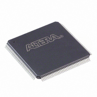
EP2C5T144C8N Altera, EP2C5T144C8N Datasheet - Page 71

EP2C5T144C8N
Manufacturer Part Number
EP2C5T144C8N
Description
IC CYCLONE II FPGA 5K 144-TQFP
Manufacturer
Altera
Series
Cyclone® IIr
Datasheet
1.EP2C5T144C8N.pdf
(168 pages)
Specifications of EP2C5T144C8N
Number Of Logic Elements/cells
4608
Number Of Labs/clbs
288
Total Ram Bits
119808
Number Of I /o
89
Voltage - Supply
1.15 V ~ 1.25 V
Mounting Type
Surface Mount
Operating Temperature
0°C ~ 85°C
Package / Case
144-TQFP, 144-VQFP
Lead Free Status / RoHS Status
Lead free / RoHS Compliant
Number Of Gates
-
Other names
544-1665
Available stocks
Company
Part Number
Manufacturer
Quantity
Price
Company:
Part Number:
EP2C5T144C8N
Manufacturer:
ALTERA
Quantity:
28
Company:
Part Number:
EP2C5T144C8N
Manufacturer:
ALTERA73
Quantity:
6 170
Part Number:
EP2C5T144C8N
Manufacturer:
ALTERA/阿尔特拉
Quantity:
20 000
Figure 2–29. EP2C15, EP2C20, EP2C35, EP2C50 & EP2C70 I/O Banks
Notes to
(1)
(2)
(3)
(4)
(5)
Altera Corporation
February 2007
& PCI-X I/O Standards
Support the 3.3-V PCI
I/O Banks 1 & 2 Also
This is a top view of the silicon die.
This is a graphic representation only. Refer to the pin list and the Quartus II software for exact pin locations.
The LVPECL I/O standard is only supported on clock input pins. This I/O standard is not supported on output
pins.
The differential SSTL-18 and SSTL-2 I/O standards are only supported on clock input pins and PLL output clock
pins.
The differential 1.8-V and 1.5-V HSTL I/O standards are only supported on clock input pins and PLL output clock
pins.
Figure
I/O Bank 2
I/O Bank 1
2–29:
Each I/O bank has its own VCCIO pins. A single device can support
1.5-V, 1.8-V, 2.5-V, and 3.3-V interfaces; each individual bank can support
a different standard with different I/O voltages. Each bank also has
dual-purpose VREF pins to support any one of the voltage-referenced
Regular I/O Block
I/O Bank 3
Bank 8
I/O Banks 7 & 8 Also Support
HSTL-18 Class II, & HSTL-15
I/O Banks 3 & 4 Also Support
HSTL-18 Class II, & HSTL-15
All I/O Banks Support
■
■
■
■
■
■
■
■
■
■
■
■
■
■
■
■
Class II I/O Standards
Class II I/O Standards
the SSTL-18 Class II,
the SSTL-18 Class II,
3.3-V LVTTL/LVCMOS
2.5-V LVTTL/LVCMOS
1.8-V LVTTL/LVCMOS
1.5-V LVCMOS
LVDS
RSDS
mini-LVDS
LVPECL (3)
SSTL-2 Class I and II
SSTL-18 Class I
HSTL-18 Class I
HSTL-15 Class I
Differential SSTL-2 (4)
Differential SSTL-18 (4)
Differential HSTL-18 (5)
Differential HSTL-15 (5)
Power Bus
Individual
Regular I/O Block
I/O Bank 4
Bank 7
Cyclone II Device Handbook, Volume 1
Notes
(1),
(2)
Cyclone II Architecture
I/O Bank 5
I/O Bank 6
I/O Banks 5 & 6 Also
Support the 3.3-V PCI
& PCI-X I/O Standards
2–59


