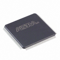
EP1C3T144C7 Altera, EP1C3T144C7 Datasheet - Page 100

EP1C3T144C7
Manufacturer Part Number
EP1C3T144C7
Description
IC CYCLONE FPGA 2910 LE 144-TQFP
Manufacturer
Altera
Series
Cyclone®r
Datasheet
1.EP1C3T144C8.pdf
(106 pages)
Specifications of EP1C3T144C7
Number Of Logic Elements/cells
2910
Number Of Labs/clbs
291
Total Ram Bits
59904
Number Of I /o
104
Voltage - Supply
1.425 V ~ 1.575 V
Mounting Type
Surface Mount
Operating Temperature
0°C ~ 85°C
Package / Case
144-TQFP, 144-VQFP
Family Name
Cyclone®
Number Of Logic Blocks/elements
2910
# I/os (max)
104
Frequency (max)
320.1MHz
Process Technology
0.13um (CMOS)
Operating Supply Voltage (typ)
1.5V
Logic Cells
2910
Ram Bits
59904
Operating Supply Voltage (min)
1.425V
Operating Supply Voltage (max)
1.575V
Operating Temp Range
0C to 85C
Operating Temperature Classification
Commercial
Mounting
Surface Mount
Pin Count
144
Package Type
TQFP
Lead Free Status / RoHS Status
Contains lead / RoHS non-compliant
Number Of Gates
-
Lead Free Status / Rohs Status
Not Compliant
Other names
544-1051
Available stocks
Company
Part Number
Manufacturer
Quantity
Price
Company:
Part Number:
EP1C3T144C7
Manufacturer:
ALTERA
Quantity:
624
Company:
Part Number:
EP1C3T144C7N
Manufacturer:
ALTERA
Quantity:
250
Part Number:
EP1C3T144C7N
Manufacturer:
ALTERA/阿尔特拉
Quantity:
20 000
Cyclone Device Handbook, Volume 1
4–30
Preliminary
Notes to
(1)
(2)
(3)
f
t
t
t
f
-
N, G0, G1, E
OUT
OUT
JITTER
LOCK
VCO
Table 4–52. Cyclone PLL Specifications (Part 2 of 2)
(to global clock)
DUTY
The t
of them are switching outputs, how much they toggle, and whether or not they use programmable current strength
or slow slew rate.
f
specification is 60 mUI.
f
operates with the specified parameters under the specified conditions.
OUT
IN/N
(3)
(1)
Table
Symbol
≥ 100 MHz. When the PLL external clock output frequency (f
JITTER
must be greater than 200 MHz to ensure correct lock detect circuit operation below –20 C. Otherwise, the PLL
specification for the PLL[2..1]_OUT pins are dependent on the I/O pins in its V
4–52:
PLL output frequency
(-6 speed grade)
PLL output frequency
(-7 speed grade)
PLL output frequency
(-8 speed grade)
Duty cycle for external clock
output (when set to 50%)
Period jitter for external clock
output
Time required to lock from end
of device configuration
PLL internal VCO operating
range
Minimum areset time
Counter values
Parameter
OUT
15.625
15.625
15.625
500.00
45.00
10.00
Min
10
—
) is smaller than 100 MHz, the jitter
1
±300
1,000
Max
405
320
275
100
32
55
—
CCIO
Altera Corporation
(2)
bank, how many
May 2008
integer
MHz
MHz
MHz
MHz
Unit
ps
μs
ns
%


