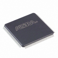
EP1C3T144C7 Altera, EP1C3T144C7 Datasheet - Page 49

EP1C3T144C7
Manufacturer Part Number
EP1C3T144C7
Description
IC CYCLONE FPGA 2910 LE 144-TQFP
Manufacturer
Altera
Series
Cyclone®r
Datasheet
1.EP1C3T144C8.pdf
(106 pages)
Specifications of EP1C3T144C7
Number Of Logic Elements/cells
2910
Number Of Labs/clbs
291
Total Ram Bits
59904
Number Of I /o
104
Voltage - Supply
1.425 V ~ 1.575 V
Mounting Type
Surface Mount
Operating Temperature
0°C ~ 85°C
Package / Case
144-TQFP, 144-VQFP
Family Name
Cyclone®
Number Of Logic Blocks/elements
2910
# I/os (max)
104
Frequency (max)
320.1MHz
Process Technology
0.13um (CMOS)
Operating Supply Voltage (typ)
1.5V
Logic Cells
2910
Ram Bits
59904
Operating Supply Voltage (min)
1.425V
Operating Supply Voltage (max)
1.575V
Operating Temp Range
0C to 85C
Operating Temperature Classification
Commercial
Mounting
Surface Mount
Pin Count
144
Package Type
TQFP
Lead Free Status / RoHS Status
Contains lead / RoHS non-compliant
Number Of Gates
-
Lead Free Status / Rohs Status
Not Compliant
Other names
544-1051
Available stocks
Company
Part Number
Manufacturer
Quantity
Price
Company:
Part Number:
EP1C3T144C7
Manufacturer:
ALTERA
Quantity:
624
Company:
Part Number:
EP1C3T144C7N
Manufacturer:
ALTERA
Quantity:
250
Part Number:
EP1C3T144C7N
Manufacturer:
ALTERA/阿尔特拉
Quantity:
20 000
Figure 2–30. Signal Path through the I/O Block
Altera Corporation
May 2008
From Logic
To Logic
Array
Array
comb_io_datain
Row or Column
io_clk[5..0]
io_cce_out
io_dataout
io_cce_in
io_datain
io_caclr
io_csclr
io_cclk
io_coe
The pin's datain signals can drive the logic array. The logic array drives
the control and data signals, providing a flexible routing resource. The
row or column IOE clocks, io_clk[5..0], provide a dedicated routing
resource for low-skew, high-speed clocks. The global clock network
generates the IOE clocks that feed the row or column I/O regions (see
“Global Clock Network and Phase-Locked Loops” on page
Figure 2–30
Each IOE contains its own control signal selection for the following
control signals: oe, ce_in, ce_out, aclr/preset, sclr/preset,
clk_in, and clk_out.
selection.
Data and
Selection
Control
Signal
illustrates the signal paths through the I/O block.
oe
ce_in
ce_out
aclr/preset
sclr
clk_in
clk_out
dataout
Figure 2–31
To Other
IOEs
illustrates the control signal
IOE
2–29).
I/O Structure
Preliminary
2–43


