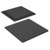
XC2V3000-5FGG676C Xilinx Inc, XC2V3000-5FGG676C Datasheet - Page 31

XC2V3000-5FGG676C
Manufacturer Part Number
XC2V3000-5FGG676C
Description
IC VIRTEX-II FPGA 3M 676-FBGA
Manufacturer
Xilinx Inc
Series
Virtex™-IIr
Datasheet
1.XC2V250-4FGG256C.pdf
(318 pages)
Specifications of XC2V3000-5FGG676C
Number Of Labs/clbs
3584
Total Ram Bits
1769472
Number Of I /o
484
Number Of Gates
3000000
Voltage - Supply
1.425 V ~ 1.575 V
Mounting Type
Surface Mount
Operating Temperature
0°C ~ 85°C
Package / Case
676-BBGA
Lead Free Status / RoHS Status
Lead free / RoHS Compliant
Number Of Logic Elements/cells
-
Other names
122-1355
Available stocks
Company
Part Number
Manufacturer
Quantity
Price
Company:
Part Number:
XC2V3000-5FGG676C
Manufacturer:
Xilinx Inc
Quantity:
10 000
- Current page: 31 of 318
- Download datasheet (3Mb)
Each block SelectRAM cell is a fully synchronous memory,
as illustrated in
inputs and outputs and are independently clocked.
Port Aspect Ratios
Table 16
18 Kbit block SelectRAM. Virtex-II block SelectRAM also
includes dedicated routing resources to provide an efficient
interface with CLBs, block SelectRAM, and multipliers.
Table 16: 18 Kbit Block SelectRAM Port Aspect Ratio
Read/Write Operations
The Virtex-II block SelectRAM read operation is fully syn-
chronous. An address is presented, and the read operation
is enabled by control signals WEA and WEB in addition to
ENA or ENB. Then, depending on clock polarity, a rising or
falling clock edge causes the stored data to be loaded into
output registers.
The write operation is also fully synchronous. Data and
address are presented, and the write operation is enabled
by control signals WEA or WEB in addition to ENA or ENB.
Then, again depending on the clock input mode, a rising or
DS031-2 (v3.5) November 5, 2007
Product Specification
Figure 30: 18 Kbit Block SelectRAM in Dual-Port Mode
Width
18
36
1
2
4
9
shows the depth and the width aspect ratios for the
16,384
Depth
8,192
4,096
2,048
1,024
512
R
Figure
DIB
DIPA
ADDRA
WEA
ENA
SSRA
DIPB
ADDRB
WEB
ENB
SSRB
DIA
Address Bus
CLKA
CLKB
ADDR[13:0]
ADDR[12:0]
ADDR[11:0]
ADDR[10:0]
18 Kbit Block SelectRAM
ADDR[9:0]
ADDR[8:0]
30. The two ports have independent
DATA[15:0]
DATA[31:0]
Data Bus
DATA[1:0]
DATA[3:0]
DATA[7:0]
DATA[0]
DOPA
DOPB
DOA
DOB
DS031_11_071602
Parity Bus
Parity[1:0]
Parity[3:0]
Parity[0]
N/A
N/A
N/A
www.xilinx.com
falling clock edge causes the data to be loaded into the
memory cell addressed.
A write operation performs a simultaneous read operation.
Three different options are available, selected by configura-
tion:
1. “WRITE_FIRST”
2. “READ_FIRST”
RAM Contents
RAM Contents
The “WRITE_FIRST” option is a transparent mode. The
same clock edge that writes the data input (DI) into the
memory also transfers DI into the output registers DO
as shown in
Data_out
The “READ_FIRST” option is a read-before-write mode.
The same clock edge that writes data input (DI) into the
memory also transfers the prior content of the memory
cell addressed into the data output registers DO, as
shown in
Data_out
Address
Address
Data_in
Data_in
Data_in
Data_in
Virtex-II Platform FPGAs: Functional Description
CLK
CLK
WE
WE
Figure 31: WRITE_FIRST Mode
Figure 32: READ_FIRST Mode
Figure
Figure
DI
DI
New
New
Old
Old
aa
aa
Internal
Internal
Memory
Memory
32.
31.
DO
DO
Data_out = Data_in
Prior stored data
New
New
New
Old
Module 2 of 4
DS031_14_102000
DS031_13_102000
23
Related parts for XC2V3000-5FGG676C
Image
Part Number
Description
Manufacturer
Datasheet
Request
R

Part Number:
Description:
IC VIRTEX-II FPGA 3M 1152-FCBGA
Manufacturer:
Xilinx Inc
Datasheet:

Part Number:
Description:
IC FPGA VIRTEX II 3M 957-FCBGA
Manufacturer:
Xilinx Inc
Datasheet:

Part Number:
Description:
IC FPGA VIRTEX-II 3M 676-FBGA
Manufacturer:
Xilinx Inc
Datasheet:

Part Number:
Description:
IC FPGA VIRTEX II 3M 957-FCBGA
Manufacturer:
Xilinx Inc
Datasheet:

Part Number:
Description:
IC FPGA VIRTEX-II 3M 1152-FBGA
Manufacturer:
Xilinx Inc
Datasheet:

Part Number:
Description:
IC FPGA VIRTEX-II 3M 1152-FBGA
Manufacturer:
Xilinx Inc
Datasheet:

Part Number:
Description:
IC FPGA VIRTEX-II 3M 676-FBGA
Manufacturer:
Xilinx Inc
Datasheet:

Part Number:
Description:
IC FPGA VIRTEX-II 3M 676-FBGA
Manufacturer:
Xilinx Inc
Datasheet:

Part Number:
Description:
IC FPGA VIRTEX-II 3M 1152-FBGA
Manufacturer:
Xilinx Inc
Datasheet:

Part Number:
Description:
IC FPGA VIRTEX-II 3M 1152-FBGA
Manufacturer:
Xilinx Inc
Datasheet:

Part Number:
Description:
IC FPGA VIRTEX-II 676FGBGA
Manufacturer:
Xilinx Inc
Datasheet:

Part Number:
Description:
IC FPGA VIRTEX-II 728PBGA
Manufacturer:
Xilinx Inc
Datasheet:

Part Number:
Description:
IC FPGA VIRTEX-II 1152FCBGA
Manufacturer:
Xilinx Inc
Datasheet:

Part Number:
Description:
IC FPGA VIRTEX-II 957FCBGA
Manufacturer:
Xilinx Inc
Datasheet:

Part Number:
Description:
IC FPGA VIRTEX-II 957FCBGA
Manufacturer:
Xilinx Inc
Datasheet:


