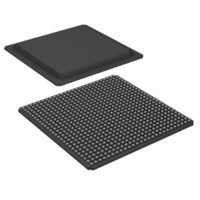
XC2V3000-5FGG676C Xilinx Inc, XC2V3000-5FGG676C Datasheet - Page 71

XC2V3000-5FGG676C
Manufacturer Part Number
XC2V3000-5FGG676C
Description
IC VIRTEX-II FPGA 3M 676-FBGA
Manufacturer
Xilinx Inc
Series
Virtex™-IIr
Datasheet
1.XC2V250-4FGG256C.pdf
(318 pages)
Specifications of XC2V3000-5FGG676C
Number Of Labs/clbs
3584
Total Ram Bits
1769472
Number Of I /o
484
Number Of Gates
3000000
Voltage - Supply
1.425 V ~ 1.575 V
Mounting Type
Surface Mount
Operating Temperature
0°C ~ 85°C
Package / Case
676-BBGA
Lead Free Status / RoHS Status
Lead free / RoHS Compliant
Number Of Logic Elements/cells
-
Other names
122-1355
Available stocks
Company
Part Number
Manufacturer
Quantity
Price
Company:
Part Number:
XC2V3000-5FGG676C
Manufacturer:
Xilinx Inc
Quantity:
10 000
- Current page: 71 of 318
- Download datasheet (3Mb)
Table 25: Pipelined Multiplier Switching Characteristics
DS031-3 (v3.5) November 5, 2007
Product Specification
Data Inputs
Clock Enable
Reset
Clock to Output Pin
Clock to Pin 35
Clock to Pin 34
Clock to Pin 33
Clock to Pin 32
Clock to Pin 31
Clock to Pin 30
Clock to Pin 29
Clock to Pin 28
Clock to Pin 27
Clock to Pin 26
Clock to Pin 25
Clock to Pin 24
Clock to Pin 23
Clock to Pin 22
Clock to Pin 21
Clock to Pin 20
Clock to Pin 19
Clock to Pin 18
Clock to Pin 17
Clock to Pin 16
Clock to Pin 15
Clock to Pin 14
Clock to Pin 13
Clock to Pin 12
Clock to Pin 11
Clock to Pin 10
Clock to Pin 9
Clock to Pin 8
Clock to Pin 7
Clock to Pin 6
Clock to Pin 5
Clock to Pin 4
Clock to Pin 3
Clock to Pin 2
Clock to Pin 1
Clock to Pin 0
Setup and Hold Times Before/After Clock
R
Description
T
T
MULIDCK_RST
MULIDCK_CE
T
MULIDCK
www.xilinx.com
T
T
T
T
T
T
T
T
T
T
T
T
T
T
T
T
T
T
T
T
T
T
T
T
T
T
T
T
T
T
T
T
T
T
T
T
MULTCK_P35
MULTCK_P34
MULTCK_P33
MULTCK_P32
MULTCK_P31
MULTCK_P30
MULTCK_P29
MULTCK_P28
MULTCK_P27
MULTCK_P26
MULTCK_P25
MULTCK_P24
MULTCK_P23
MULTCK_P22
MULTCK_P21
MULTCK_P20
MULTCK_P19
MULTCK_P18
MULTCK_P17
MULTCK_P16
MULTCK_P15
MULTCK_P14
MULTCK_P13
MULTCK_P12
MULTCK_P11
MULTCK_P10
MULTCK_P9
MULTCK_P8
MULTCK_P7
MULTCK_P6
MULTCK_P5
MULTCK_P4
MULTCK_P3
MULTCK_P2
MULTCK_P1
MULTCK_P0
Symbol
Virtex-II Platform FPGAs: DC and Switching Characteristics
/T
/T
/T
MULCKID
MULCKID_CE
MULCKID_RST
3.00/ 0.00
0.72/ 0.00
0.72/ 0.00
3.05
2.95
2.85
2.76
2.66
2.56
2.47
2.37
2.27
2.17
2.08
1.98
1.88
1.79
1.69
1.59
1.50
1.40
1.30
1.20
1.11
1.01
0.91
0.91
0.91
0.91
0.91
0.91
0.91
0.91
0.91
0.91
0.91
0.91
0.91
0.91
-6
Speed Grade
3.45/ 0.00
0.80/ 0.00
0.80/ 0.00
6.91
6.75
6.59
6.43
6.27
6.11
5.95
5.79
5.63
5.47
5.31
5.15
4.99
4.83
4.67
4.51
4.35
4.19
4.03
3.87
3.71
3.55
3.39
3.23
3.07
2.91
2.75
2.59
2.43
2.27
2.11
1.95
1.79
1.63
1.47
1.31
-5
3.89/ 0.00
0.86/ 0.00
0.86/ 0.00
8.12
7.93
7.74
7.56
7.37
7.19
7.00
6.81
6.63
6.44
6.26
6.07
5.88
5.70
5.51
5.33
5.14
4.95
4.77
4.58
4.40
4.21
4.02
3.84
3.65
3.47
3.28
3.09
2.91
2.72
2.54
2.35
2.16
1.98
1.79
1.61
-4
Module 3 of 4
ns, Max
ns, Max
ns, Max
ns, Max
ns, Max
ns, Max
ns, Max
ns, Max
ns, Max
ns, Max
ns, Max
ns, Max
ns, Max
ns, Max
ns, Max
ns, Max
ns, Max
ns, Max
ns, Max
ns, Max
ns, Max
ns, Max
ns, Max
ns, Max
ns, Max
ns, Max
ns, Max
ns, Max
ns, Max
ns, Max
ns, Max
ns, Max
ns, Max
ns, Max
ns, Max
ns, Max
ns, Max
ns, Max
ns, Max
Units
23
Related parts for XC2V3000-5FGG676C
Image
Part Number
Description
Manufacturer
Datasheet
Request
R

Part Number:
Description:
IC VIRTEX-II FPGA 3M 1152-FCBGA
Manufacturer:
Xilinx Inc
Datasheet:

Part Number:
Description:
IC FPGA VIRTEX II 3M 957-FCBGA
Manufacturer:
Xilinx Inc
Datasheet:

Part Number:
Description:
IC FPGA VIRTEX-II 3M 676-FBGA
Manufacturer:
Xilinx Inc
Datasheet:

Part Number:
Description:
IC FPGA VIRTEX II 3M 957-FCBGA
Manufacturer:
Xilinx Inc
Datasheet:

Part Number:
Description:
IC FPGA VIRTEX-II 3M 1152-FBGA
Manufacturer:
Xilinx Inc
Datasheet:

Part Number:
Description:
IC FPGA VIRTEX-II 3M 1152-FBGA
Manufacturer:
Xilinx Inc
Datasheet:

Part Number:
Description:
IC FPGA VIRTEX-II 3M 676-FBGA
Manufacturer:
Xilinx Inc
Datasheet:

Part Number:
Description:
IC FPGA VIRTEX-II 3M 676-FBGA
Manufacturer:
Xilinx Inc
Datasheet:

Part Number:
Description:
IC FPGA VIRTEX-II 3M 1152-FBGA
Manufacturer:
Xilinx Inc
Datasheet:

Part Number:
Description:
IC FPGA VIRTEX-II 3M 1152-FBGA
Manufacturer:
Xilinx Inc
Datasheet:

Part Number:
Description:
IC FPGA VIRTEX-II 676FGBGA
Manufacturer:
Xilinx Inc
Datasheet:

Part Number:
Description:
IC FPGA VIRTEX-II 728PBGA
Manufacturer:
Xilinx Inc
Datasheet:

Part Number:
Description:
IC FPGA VIRTEX-II 1152FCBGA
Manufacturer:
Xilinx Inc
Datasheet:

Part Number:
Description:
IC FPGA VIRTEX-II 957FCBGA
Manufacturer:
Xilinx Inc
Datasheet:

Part Number:
Description:
IC FPGA VIRTEX-II 957FCBGA
Manufacturer:
Xilinx Inc
Datasheet:


