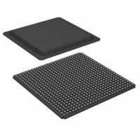
XC2V3000-5FGG676C Xilinx Inc, XC2V3000-5FGG676C Datasheet - Page 36

XC2V3000-5FGG676C
Manufacturer Part Number
XC2V3000-5FGG676C
Description
IC VIRTEX-II FPGA 3M 676-FBGA
Manufacturer
Xilinx Inc
Series
Virtex™-IIr
Datasheet
1.XC2V250-4FGG256C.pdf
(318 pages)
Specifications of XC2V3000-5FGG676C
Number Of Labs/clbs
3584
Total Ram Bits
1769472
Number Of I /o
484
Number Of Gates
3000000
Voltage - Supply
1.425 V ~ 1.575 V
Mounting Type
Surface Mount
Operating Temperature
0°C ~ 85°C
Package / Case
676-BBGA
Lead Free Status / RoHS Status
Lead free / RoHS Compliant
Number Of Logic Elements/cells
-
Other names
122-1355
Available stocks
Company
Part Number
Manufacturer
Quantity
Price
Company:
Part Number:
XC2V3000-5FGG676C
Manufacturer:
Xilinx Inc
Quantity:
10 000
- Current page: 36 of 318
- Download datasheet (3Mb)
The most common configuration option of this element is as
a buffer. A BUFG function in this (global buffer) mode, is
shown in
The Virtex-II global clock buffer BUFG can also be config-
ured as a clock enable/disable circuit
a two-input clock multiplexer
description of these two options is provided below. Each of
DS031-2 (v3.5) November 5, 2007
Product Specification
Figure 39: Virtex-II Clock Distribution Configurations
Figure
Clock Distribution
Figure 41: Virtex-II BUFG Function
R
Buffer
Clock
Clock
Pad
41.
I
0
I
BUFG
NW
SW
DS031_61_101200
(Figure
8 BUFGMUX
16 Clocks
8 BUFGMUX
O
Clock Distribution
(Figure
CLKOUT
Buffer
DS031_43_101000
CLKIN
DCM
Clock
Clock
43). A functional
Pad
Figure 40: Virtex-II Clock Distribution
I
0
42), as well as
SE
NE
www.xilinx.com
NW
SW
Global clock buffers are used to distribute the clock to some
or all synchronous logic elements (such as registers in
CLBs and IOBs, and SelectRAM blocks.
Eight global clocks can be used in each quadrant of the
Virtex-II device. Designers should consider the clock distri-
bution detail of the device prior to pin-locking and floorplan-
ning (see the Virtex-II User Guide).
Figure 40
In each quadrant, up to eight clocks are organized in clock
rows. A clock row supports up to 16 CLB rows (eight up and
eight down). For the largest devices a new clock row is
added, as necessary.
To reduce power consumption, any unused clock branches
remain static.
Global clocks are driven by dedicated clock buffers (BUFG),
which can also be used to gate the clock (BUFGCE) or to mul-
tiplex between two independent clock inputs (BUFGMUX).
them can be used in either of two modes, selected by con-
figuration: rising clock edge or falling clock edge.
This section describes the rising clock edge option. For the
opposite option, falling clock edge, just change all "rising"
references to "falling" and all "High" references to "Low",
except for the description of the CE or S levels. The rising
clock edge option uses the BUFGCE and BUFGMUX prim-
itives. The falling clock edge option uses the BUFGCE_1
and BUFGMUX_1 primitives.
BUFGCE
If the CE input is active (High) prior to the incoming rising
clock edge, this Low-to-High-to-Low clock pulse passes
through the clock buffer. Any level change of CE during the
incoming clock High time has no effect.
8
8
8 BUFGMUX
8 BUFGMUX
Virtex-II Platform FPGAs: Functional Description
16 Clocks
shows clock distribution in Virtex-II devices.
8
8
DS031_45_120200
8 max
SE
NE
Module 2 of 4
28
Related parts for XC2V3000-5FGG676C
Image
Part Number
Description
Manufacturer
Datasheet
Request
R

Part Number:
Description:
IC VIRTEX-II FPGA 3M 1152-FCBGA
Manufacturer:
Xilinx Inc
Datasheet:

Part Number:
Description:
IC FPGA VIRTEX II 3M 957-FCBGA
Manufacturer:
Xilinx Inc
Datasheet:

Part Number:
Description:
IC FPGA VIRTEX-II 3M 676-FBGA
Manufacturer:
Xilinx Inc
Datasheet:

Part Number:
Description:
IC FPGA VIRTEX II 3M 957-FCBGA
Manufacturer:
Xilinx Inc
Datasheet:

Part Number:
Description:
IC FPGA VIRTEX-II 3M 1152-FBGA
Manufacturer:
Xilinx Inc
Datasheet:

Part Number:
Description:
IC FPGA VIRTEX-II 3M 1152-FBGA
Manufacturer:
Xilinx Inc
Datasheet:

Part Number:
Description:
IC FPGA VIRTEX-II 3M 676-FBGA
Manufacturer:
Xilinx Inc
Datasheet:

Part Number:
Description:
IC FPGA VIRTEX-II 3M 676-FBGA
Manufacturer:
Xilinx Inc
Datasheet:

Part Number:
Description:
IC FPGA VIRTEX-II 3M 1152-FBGA
Manufacturer:
Xilinx Inc
Datasheet:

Part Number:
Description:
IC FPGA VIRTEX-II 3M 1152-FBGA
Manufacturer:
Xilinx Inc
Datasheet:

Part Number:
Description:
IC FPGA VIRTEX-II 676FGBGA
Manufacturer:
Xilinx Inc
Datasheet:

Part Number:
Description:
IC FPGA VIRTEX-II 728PBGA
Manufacturer:
Xilinx Inc
Datasheet:

Part Number:
Description:
IC FPGA VIRTEX-II 1152FCBGA
Manufacturer:
Xilinx Inc
Datasheet:

Part Number:
Description:
IC FPGA VIRTEX-II 957FCBGA
Manufacturer:
Xilinx Inc
Datasheet:

Part Number:
Description:
IC FPGA VIRTEX-II 957FCBGA
Manufacturer:
Xilinx Inc
Datasheet:


