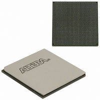
EP2SGX60EF1152C3N Altera, EP2SGX60EF1152C3N Datasheet - Page 143

EP2SGX60EF1152C3N
Manufacturer Part Number
EP2SGX60EF1152C3N
Description
IC STRATIX II GX 60K 1152-FBGA
Manufacturer
Altera
Series
Stratix® II GXr
Datasheet
1.EP2SGX30DF780C5.pdf
(316 pages)
Specifications of EP2SGX60EF1152C3N
Number Of Logic Elements/cells
60440
Number Of Labs/clbs
3022
Total Ram Bits
2544192
Number Of I /o
534
Voltage - Supply
1.15 V ~ 1.25 V
Mounting Type
Surface Mount
Operating Temperature
0°C ~ 85°C
Package / Case
1152-FBGA
Lead Free Status / RoHS Status
Lead free / RoHS Compliant
Number Of Gates
-
Other names
544-2181
Available stocks
Company
Part Number
Manufacturer
Quantity
Price
Company:
Part Number:
EP2SGX60EF1152C3N
Manufacturer:
ATMEL
Quantity:
1 420
- Current page: 143 of 316
- Download datasheet (2Mb)
Altera Corporation
October 2007
Notes to
(1)
(2)
(3)
(4)
(5)
(6)
VCCSEL
(V
VCCSEL
(V
VCCSEL
by V
Stratix II GX Always
Table 2–36. Board Design Recommendations for nCEO and nCE Input Buffer Power
Table 2–37. Supported TDO/TDI Voltage Combinations (Part 1 of 2)
nCE Input Buffer Power in
C C I O
C C I O
Device
C C P D
Input buffer is 3.3-V tolerant.
The nCEO output buffer meets V
Input buffer is 2.5-V tolerant.
The nCEO output buffer meets V
Input buffer is 1.8-V tolerant.
An external 250-Ω pull-up resistor is not required, but recommended if signal levels on the board are not optimal.
Bank 3 = 1.5 V)
Bank 3 = 1.8 V)
I/O Bank 3
Table
low (nCE powered
high
high
= 3.3 V)
V
Buffer Power
2–36:
C C P D
TDI Input
(3.3 V)
Table 2–36
can successfully drive nCE for all power supply combinations.
For JTAG chains, the TDO pin of the first device drives the TDI pin of the
second device in the chain. The V
(TCK, TMS, TDI, and TRST) is internally hardwired to GND selecting the
3.3-V/2.5-V input buffer powered by V
V
TDI on the second device, but that may not be possible depending on the
application.
ensure proper JTAG chain operation.
V
V
C C I O
CCIO
v
C C I O
v
v
(1),
O H
OH
(1),
v
= 3.3 V V
of the TDO bank from the first device match the V
= 3.3 V
(MIN) = 2.0 V.
(1)
(MIN) = 2.4 V.
(2)
(2)
contains board design recommendations to ensure that nCEO
Table 2–37
Stratix II GX nCEO V
Stratix II GX TDO V
C C I O
V
v
v
C C I O
v
(3),
(3),
v
= 2.5 V
(4)
= 2.5 V
(2)
(4)
(4)
contains board design recommendations to
V
C C I O
CCIO
C C I O
V
C C I O
CCSEL
v
v
Stratix II GX Device Handbook, Volume 1
Voltage Level in I/O Bank 4
Voltage Level in I/O Bank 7
v
v
= 1.8 V V
(5)
(6)
= 1.8 V V
(3)
input on the JTAG input I/O cells
CCPD
. The ideal case is to have the
Level shifter
C C I O
Level shifter
required
C C I O
required
Stratix II GX Architecture
v
v
= 1.5 V V
= 1.5 V V
CCSEL
Level shifter
Level shifter
C C I O
Level shifter
C C I O
settings for
required
required
required
v
= 1.2 V
= 1.2 V
2–135
Related parts for EP2SGX60EF1152C3N
Image
Part Number
Description
Manufacturer
Datasheet
Request
R

Part Number:
Description:
4. Serial Configuration Devices Epcs1, Epcs4, Epcs16, Epcs64, And Epcs128 Data Sheet
Manufacturer:
Altera Corporation
Datasheet:

Part Number:
Description:
CYCLONE II STARTER KIT EP2C20N
Manufacturer:
Altera
Datasheet:

Part Number:
Description:
CPLD, EP610 Family, ECMOS Process, 300 Gates, 16 Macro Cells, 16 Reg., 16 User I/Os, 5V Supply, 35 Speed Grade, 24DIP
Manufacturer:
Altera Corporation
Datasheet:

Part Number:
Description:
CPLD, EP610 Family, ECMOS Process, 300 Gates, 16 Macro Cells, 16 Reg., 16 User I/Os, 5V Supply, 15 Speed Grade, 24DIP
Manufacturer:
Altera Corporation
Datasheet:

Part Number:
Description:
Manufacturer:
Altera Corporation
Datasheet:

Part Number:
Description:
CPLD, EP610 Family, ECMOS Process, 300 Gates, 16 Macro Cells, 16 Reg., 16 User I/Os, 5V Supply, 30 Speed Grade, 24DIP
Manufacturer:
Altera Corporation
Datasheet:

Part Number:
Description:
High-performance, low-power erasable programmable logic devices with 8 macrocells, 10ns
Manufacturer:
Altera Corporation
Datasheet:

Part Number:
Description:
High-performance, low-power erasable programmable logic devices with 8 macrocells, 7ns
Manufacturer:
Altera Corporation
Datasheet:

Part Number:
Description:
Classic EPLD
Manufacturer:
Altera Corporation
Datasheet:

Part Number:
Description:
High-performance, low-power erasable programmable logic devices with 8 macrocells, 10ns
Manufacturer:
Altera Corporation
Datasheet:

Part Number:
Description:
Manufacturer:
Altera Corporation
Datasheet:

Part Number:
Description:
Manufacturer:
Altera Corporation
Datasheet:

Part Number:
Description:
Manufacturer:
Altera Corporation
Datasheet:


