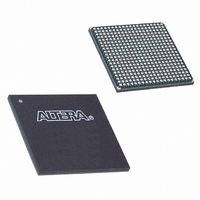
EP1C4F400C7 Altera, EP1C4F400C7 Datasheet - Page 28

EP1C4F400C7
Manufacturer Part Number
EP1C4F400C7
Description
IC CYCLONE FPGA 4K LE 400-FBGA
Manufacturer
Altera
Series
Cyclone®r
Datasheet
1.EP1C3T144C8.pdf
(106 pages)
Specifications of EP1C4F400C7
Number Of Logic Elements/cells
4000
Number Of Labs/clbs
400
Total Ram Bits
78336
Number Of I /o
301
Voltage - Supply
1.425 V ~ 1.575 V
Mounting Type
Surface Mount
Operating Temperature
0°C ~ 85°C
Package / Case
400-FBGA
Family Name
Cyclone®
Number Of Logic Blocks/elements
4000
# I/os (max)
301
Frequency (max)
320.1MHz
Process Technology
0.13um (CMOS)
Operating Supply Voltage (typ)
1.5V
Logic Cells
4000
Ram Bits
78336
Operating Supply Voltage (min)
1.425V
Operating Supply Voltage (max)
1.575V
Operating Temp Range
0C to 85C
Operating Temperature Classification
Commercial
Mounting
Surface Mount
Pin Count
400
Package Type
FBGA
Lead Free Status / RoHS Status
Contains lead / RoHS non-compliant
Number Of Gates
-
Lead Free Status / Rohs Status
Not Compliant
Other names
544-2079
Available stocks
Company
Part Number
Manufacturer
Quantity
Price
Company:
Part Number:
EP1C4F400C7
Manufacturer:
TI
Quantity:
150
Company:
Part Number:
EP1C4F400C7
Manufacturer:
ALTERA
Quantity:
3 000
Company:
Part Number:
EP1C4F400C7N
Manufacturer:
ALTERA
Quantity:
784
Part Number:
EP1C4F400C7N
Manufacturer:
ALTERA
Quantity:
20 000
Cyclone Device Handbook, Volume 1
2–22
Preliminary
4K
2K
1K
512
256
128
512
256
128
4K
2K
1K
512
256
512
256
Table 2–3. M4K RAM Block Configurations (Simple Dual-Port)
Table 2–4. M4K RAM Block Configurations (True Dual-Port)
Read Port
×
×
×
×
×
×
×
×
×
×
×
×
×
×
×
×
1
2
4
1
2
4
8
16
32
9
18
36
8
16
9
18
Port A
4K × 1 2K × 2 1K × 4 512 × 8
v
v
v
v
v
v
—
—
—
4K × 1
v
v
v
v
v
v
—
—
—
is not available in the true dual-port mode. Mixed-width configurations
are also possible, allowing different read and write widths.
and
When the M4K RAM block is configured as a shift register block, you can
create a shift register up to 4,608 bits (w × m × n).
v
v
v
v
v
—
—
2–4
v
v
v
v
v
v
—
—
—
summarize the possible M4K RAM block configurations.
2K × 2
v
v
v
v
v
—
—
v
v
v
v
v
v
—
—
—
1K × 4
v
v
v
v
v
—
—
256 × 16
Write Port
v
v
v
v
v
v
—
—
—
512 × 8
Port B
v
v
v
v
v
—
—
128 × 32
v
v
v
v
v
v
—
—
—
256 × 16
v
v
v
v
v
—
—
512 × 9 256 × 18 128 × 36
v
v
v
—
—
—
—
—
—
512 × 9
Altera Corporation
v
v
—
—
—
—
—
v
v
v
—
—
—
—
—
—
Tables 2–3
256 × 18
May 2008
v
v
—
—
—
—
—
v
v
v
—
—
—
—
—
—


