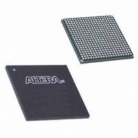
EP1C4F400C7 Altera, EP1C4F400C7 Datasheet - Page 98

EP1C4F400C7
Manufacturer Part Number
EP1C4F400C7
Description
IC CYCLONE FPGA 4K LE 400-FBGA
Manufacturer
Altera
Series
Cyclone®r
Datasheet
1.EP1C3T144C8.pdf
(106 pages)
Specifications of EP1C4F400C7
Number Of Logic Elements/cells
4000
Number Of Labs/clbs
400
Total Ram Bits
78336
Number Of I /o
301
Voltage - Supply
1.425 V ~ 1.575 V
Mounting Type
Surface Mount
Operating Temperature
0°C ~ 85°C
Package / Case
400-FBGA
Family Name
Cyclone®
Number Of Logic Blocks/elements
4000
# I/os (max)
301
Frequency (max)
320.1MHz
Process Technology
0.13um (CMOS)
Operating Supply Voltage (typ)
1.5V
Logic Cells
4000
Ram Bits
78336
Operating Supply Voltage (min)
1.425V
Operating Supply Voltage (max)
1.575V
Operating Temp Range
0C to 85C
Operating Temperature Classification
Commercial
Mounting
Surface Mount
Pin Count
400
Package Type
FBGA
Lead Free Status / RoHS Status
Contains lead / RoHS non-compliant
Number Of Gates
-
Lead Free Status / Rohs Status
Not Compliant
Other names
544-2079
Available stocks
Company
Part Number
Manufacturer
Quantity
Price
Company:
Part Number:
EP1C4F400C7
Manufacturer:
TI
Quantity:
150
Company:
Part Number:
EP1C4F400C7
Manufacturer:
ALTERA
Quantity:
3 000
Company:
Part Number:
EP1C4F400C7N
Manufacturer:
ALTERA
Quantity:
784
Part Number:
EP1C4F400C7N
Manufacturer:
ALTERA
Quantity:
20 000
Cyclone Device Handbook, Volume 1
4–28
Preliminary
Tables 4–50
and row pins in Cyclone devices.
Note to
(1)
Note to
(1)
LVTTL
2.5 V
1.8 V
1.5 V
LVCMOS
SSTL-3 class I
SSTL-3 class II
SSTL-2 class I
SSTL-2 class II
3.3-V PCI
LVDS
LVTTL
2.5 V
1.8 V
1.5 V
LVCMOS
SSTL-3 class I
SSTL-3 class II
SSTL-2 class I
SSTL-2 class II
LVDS
Table 4–49. Cyclone Maximum Input Clock Rate for Row Pins
Table 4–50. Cyclone Maximum Output Clock Rate for Column Pins
EP1C3 devices do not support the PCI I/O standard. These parameters are only
available on row I/O pins.
EP1C3 devices do not support the PCI I/O standard.
I/O Standard
I/O Standard
Tables 4–48
Table
(1)
and
4–50:
4–51
through 4–49:
show the maximum output clock rate for column
-6 Speed
-6 Speed
Grade
Grade
464
392
387
387
405
405
414
464
473
464
567
304
220
213
166
304
100
100
134
134
320
-7 Speed
-7 Speed
Grade
Grade
428
302
311
320
374
356
365
428
432
428
549
304
220
213
166
304
100
100
134
134
320
-8 Speed
-8 Speed
Grade
Grade
Altera Corporation
387
207
252
243
333
293
302
396
396
387
531
304
220
213
166
304
100
100
134
134
275
May 2008
MHz
MHz
MHz
MHz
MHz
MHz
MHz
MHz
MHz
MHz
MHz
MHz
MHz
MHz
MHz
MHz
MHz
MHz
MHz
MHz
MHz
Unit
Unit


