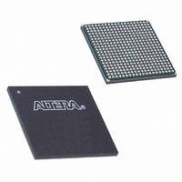
EP1C4F400C7 Altera, EP1C4F400C7 Datasheet - Page 50

EP1C4F400C7
Manufacturer Part Number
EP1C4F400C7
Description
IC CYCLONE FPGA 4K LE 400-FBGA
Manufacturer
Altera
Series
Cyclone®r
Datasheet
1.EP1C3T144C8.pdf
(106 pages)
Specifications of EP1C4F400C7
Number Of Logic Elements/cells
4000
Number Of Labs/clbs
400
Total Ram Bits
78336
Number Of I /o
301
Voltage - Supply
1.425 V ~ 1.575 V
Mounting Type
Surface Mount
Operating Temperature
0°C ~ 85°C
Package / Case
400-FBGA
Family Name
Cyclone®
Number Of Logic Blocks/elements
4000
# I/os (max)
301
Frequency (max)
320.1MHz
Process Technology
0.13um (CMOS)
Operating Supply Voltage (typ)
1.5V
Logic Cells
4000
Ram Bits
78336
Operating Supply Voltage (min)
1.425V
Operating Supply Voltage (max)
1.575V
Operating Temp Range
0C to 85C
Operating Temperature Classification
Commercial
Mounting
Surface Mount
Pin Count
400
Package Type
FBGA
Lead Free Status / RoHS Status
Contains lead / RoHS non-compliant
Number Of Gates
-
Lead Free Status / Rohs Status
Not Compliant
Other names
544-2079
Available stocks
Company
Part Number
Manufacturer
Quantity
Price
Company:
Part Number:
EP1C4F400C7
Manufacturer:
TI
Quantity:
150
Company:
Part Number:
EP1C4F400C7
Manufacturer:
ALTERA
Quantity:
3 000
Company:
Part Number:
EP1C4F400C7N
Manufacturer:
ALTERA
Quantity:
784
Part Number:
EP1C4F400C7N
Manufacturer:
ALTERA
Quantity:
20 000
Cyclone Device Handbook, Volume 1
Figure 2–31. Control Signal Selection per IOE
2–44
Preliminary
Dedicated I/O
Clock [5..0]
Local
Interconnect
Local
Interconnect
Local
Interconnect
Local
Interconnect
Local
Interconnect
Local
Interconnect
io_coe
io_csclr
io_caclr
io_cce_out
io_cce_in
io_cclk
In normal bidirectional operation, you can use the input register for input
data requiring fast setup times. The input register can have its own clock
input and clock enable separate from the OE and output registers. The
output register can be used for data requiring fast clock-to-output
performance. The OE register is available for fast clock-to-output enable
timing. The OE and output register share the same clock source and the
same clock enable source from the local interconnect in the associated
LAB, dedicated I/O clocks, or the column and row interconnects.
Figure 2–32
shows the IOE in bidirectional configuration.
clk_in
clk_out
ce_in
ce_out
aclr/preset
Altera Corporation
sclr/preset
May 2008
oe


