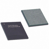
EP3C25F324I7N Altera, EP3C25F324I7N Datasheet - Page 22

EP3C25F324I7N
Manufacturer Part Number
EP3C25F324I7N
Description
IC CYCLONE III FPGA 25K 324 FBGA
Manufacturer
Altera
Series
Cyclone® IIIr
Datasheets
1.EP3C5F256C8N.pdf
(5 pages)
2.EP3C5F256C8N.pdf
(34 pages)
3.EP3C5F256C8N.pdf
(66 pages)
4.EP3C5F256C8N.pdf
(14 pages)
5.EP3C5F256C8N.pdf
(76 pages)
6.EP3C25F324I7N.pdf
(274 pages)
Specifications of EP3C25F324I7N
Number Of Logic Elements/cells
24624
Number Of Labs/clbs
1539
Total Ram Bits
608256
Number Of I /o
215
Voltage - Supply
1.15 V ~ 1.25 V
Mounting Type
Surface Mount
Operating Temperature
-40°C ~ 100°C
Package / Case
324-FBGA
Family Name
Cyclone III
Number Of Logic Blocks/elements
24624
# I/os (max)
215
Frequency (max)
437.5MHz
Process Technology
65nm
Operating Supply Voltage (typ)
1.2V
Logic Cells
24624
Ram Bits
608256
Operating Supply Voltage (min)
1.15V
Operating Supply Voltage (max)
1.25V
Operating Temp Range
-40C to 100C
Operating Temperature Classification
Industrial
Mounting
Surface Mount
Pin Count
324
Package Type
FBGA
For Use With
544-2601 - KIT DEV CYCLONE III LS EP3CLS200544-2411 - KIT DEV NIOS II CYCLONE III ED.544-2370 - KIT STARTER CYCLONE III EP3C25
Lead Free Status / RoHS Status
Lead free / RoHS Compliant
Number Of Gates
-
Lead Free Status / Rohs Status
Compliant
Other names
544-2544
Available stocks
Company
Part Number
Manufacturer
Quantity
Price
Company:
Part Number:
EP3C25F324I7N
Manufacturer:
ALTERA32
Quantity:
181
Page 22
Table 8. Requirement and Behavior of Device during Various Power-up Stages
Pre-Power Up
V
POR
CC
Ramp
Stages
f
After the Cyclone III device enters user mode, the POR circuit continues to monitor
the VCCINT and VCCA pins so that a brown-out condition during user mode can be
detected. If the V
mode, the POR circuit resets the device. The POR circuit does not reset the device if
the V
For more information about power-on reset, refer to the
Reset in Cyclone III Devices
Signals can be driven into
Cyclone III I/O pins, dedicated
inputs and dedicated clock pins
without damaging the device.
Determine the required POR time
for your device; fast POR (3 ms to
9 ms) or standard POR (50 ms to
200 ms). Selection is determined
by
Can support any power-up
sequence of supplies.
V
required. V
configuration pins (1, 6, 7, and 8)
are required.
Supplies must meet ramp rate
according to required POR; 50 µs
to 3 ms for fast POR or 50 ms for
standard POR. Fast POR is used
when Cyclone III device is
required to wake up quickly to
begin operation. Select POR using
MSEL
Configuring Cyclone III Devices
chapter in volume 1 of the
Cyclone III Device Handbook.
V
operating voltage level.
If maximum V
be met, use an external
component to hold
until the power supplies have
reached their minimum
recommended operating levels.
Else, the device may not configure
properly and enter user mode.
Maintain V
C C IO
CC
MSEL
ramp must be monotonic.
CCIO
, V
pin settings. Refer to the
C C IN T
pins setting.
voltage sags during user mode.
Requirement
C C
C CI O
, and V
ramp to desired
C C
for banks with
ramp time cannot
CCINT
nCONFIG
C C A
are
and V
chapter in volume 1 of the Cyclone III Device Handbook.
low
CCA
voltage sags below the POR trip point during user
Not applicable
Output buffers tri-stated for all conditions, for example:
■
■
■
Exception for configuration pins, which are expected to drive
out during power-up cycle. No hot socketing circuit for these
pins.
No current path exists from I/O pin to V
hot-socketing circuit is enabled. Refer to the
and Power-On Reset
Device Handbook for leakage or driving current during
hot-socketing.
Safe from latch-up, no low-impedance path from V
that may result in large current passing through the path.
Output buffers remain tri-stated.
POR circuit keeps device in reset state until all V
have stabilized and reached acceptable levels before
configuration is triggered.
when V
if the I/O pad voltage is higher than V
sudden voltage spikes (overshoot) during hot-socketing.
Setup
CC I O
is powered before V
chapter in volume 1 of the Cyclone III
Behavior
Hot Socketing and Power-On
© November 2008 Altera Corporation
C C I N T
Board Design Considerations
C C IN T
CC I O
or V
Hot Socketing
CC
C CI O
supplies
C C
, as
to GND


