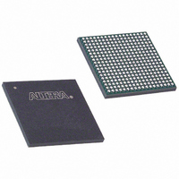
EP3C25F324I7N Altera, EP3C25F324I7N Datasheet - Page 24

EP3C25F324I7N
Manufacturer Part Number
EP3C25F324I7N
Description
IC CYCLONE III FPGA 25K 324 FBGA
Manufacturer
Altera
Series
Cyclone® IIIr
Datasheets
1.EP3C5F256C8N.pdf
(5 pages)
2.EP3C5F256C8N.pdf
(34 pages)
3.EP3C5F256C8N.pdf
(66 pages)
4.EP3C5F256C8N.pdf
(14 pages)
5.EP3C5F256C8N.pdf
(76 pages)
6.EP3C25F324I7N.pdf
(274 pages)
Specifications of EP3C25F324I7N
Number Of Logic Elements/cells
24624
Number Of Labs/clbs
1539
Total Ram Bits
608256
Number Of I /o
215
Voltage - Supply
1.15 V ~ 1.25 V
Mounting Type
Surface Mount
Operating Temperature
-40°C ~ 100°C
Package / Case
324-FBGA
Family Name
Cyclone III
Number Of Logic Blocks/elements
24624
# I/os (max)
215
Frequency (max)
437.5MHz
Process Technology
65nm
Operating Supply Voltage (typ)
1.2V
Logic Cells
24624
Ram Bits
608256
Operating Supply Voltage (min)
1.15V
Operating Supply Voltage (max)
1.25V
Operating Temp Range
-40C to 100C
Operating Temperature Classification
Industrial
Mounting
Surface Mount
Pin Count
324
Package Type
FBGA
For Use With
544-2601 - KIT DEV CYCLONE III LS EP3CLS200544-2411 - KIT DEV NIOS II CYCLONE III ED.544-2370 - KIT STARTER CYCLONE III EP3C25
Lead Free Status / RoHS Status
Lead free / RoHS Compliant
Number Of Gates
-
Lead Free Status / Rohs Status
Compliant
Other names
544-2544
Available stocks
Company
Part Number
Manufacturer
Quantity
Price
Company:
Part Number:
EP3C25F324I7N
Manufacturer:
ALTERA32
Quantity:
181
Page 24
f
f
JTAG/Configuration Chain Connection
Connect the JTAG pins of the device to the download cable header correctly. If you
have more than one device in the chain, connect the TDO pin of a device to the TDI pin
of the next device in the chain.
All I/O inputs must maintain a maximum AC voltage of 4.1 V. Because JTAG pins do
not have the internal PCI clamping diodes to prevent voltage overshoot when using
V
2.5 V supply from V
power up the download cable's V
For more information on JTAG configuration chain, refer to the
Devices
the FPGA devices in chain in other configuration schemes such as AS, AP, PS, and
FPP.
Multi Device Multi VCCIO (Level Shifter)
The operating voltage supplied to the Altera download cable by the target board
through the 10-pin header determines the I/O voltage level of the download cable.
The JTAG pins for all Cyclone III devices reside in Bank 1 and their I/O standard
support is controlled by the V
As the download cable interfaces with the JTAG pins of your device, ensure that the
download cable I/O voltage and the JTAG pin voltage are compatible.
the I/O voltages supported by different download cables.
Table 9. Download Cable I/O Voltage
For more information about JTAG configuration with Altera download cables, refer to
the
Handbook, and the appropriate download cable user guide.
Notes to
(1) When interfacing the download cables with the Cyclone III device, you must ensure that
(2) When using device V
USB-Blaster
ByteBlaster
ByteBlasterMV
MasterBlaster
CCIO
Download Cable
Configuring Cyclone III Devices
all I/O inputs to the device maintain a maximum AC voltage of 4.1 V. Altera recommends
powering up the download cables with V
3.3 V on your Cyclone III devices.
V
supply voltage of 1.2 V.
CC
of 2.5 V, 3.0 V or 3.3 V, you must power up the download cable's V
with the supply from V
chapter in volume 1 of the Cyclone III Device Handbook. You can also cascade
Table
TM
TM
TM
9:
II
TM
CCIO
2.5 V V
CCA
of 1.2 V, 1.5 V, or 1.8 V, you can power up the download cable's
. When using device V
CCIO
v
v
v
v
CCA
. However, Altera download cables do not support a target
(1)
CCIO
CCA
CC
chapter in volume 1 of the Cyclone III Device
setting for Bank 1.
of 2.5 V when using V
with the supply from V
1.8 V V
I/O Voltage
v
v
—
—
CCIO
CCIO
(2)
of 1.2 V, 1.5 V, or 1.8 V, you can
CCIO
1.5 V V
of 2.5 V, 3.0 V, or
© November 2008 Altera Corporation
v
—
—
—
CCIO
CCIO
Configuring Cyclone III
.
(2)
Board Design Considerations
Table 9
CC
with a
shows


