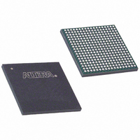
EP3C25F324I7N Altera, EP3C25F324I7N Datasheet - Page 42

EP3C25F324I7N
Manufacturer Part Number
EP3C25F324I7N
Description
IC CYCLONE III FPGA 25K 324 FBGA
Manufacturer
Altera
Series
Cyclone® IIIr
Datasheets
1.EP3C5F256C8N.pdf
(5 pages)
2.EP3C5F256C8N.pdf
(34 pages)
3.EP3C5F256C8N.pdf
(66 pages)
4.EP3C5F256C8N.pdf
(14 pages)
5.EP3C5F256C8N.pdf
(76 pages)
6.EP3C25F324I7N.pdf
(274 pages)
Specifications of EP3C25F324I7N
Number Of Logic Elements/cells
24624
Number Of Labs/clbs
1539
Total Ram Bits
608256
Number Of I /o
215
Voltage - Supply
1.15 V ~ 1.25 V
Mounting Type
Surface Mount
Operating Temperature
-40°C ~ 100°C
Package / Case
324-FBGA
Family Name
Cyclone III
Number Of Logic Blocks/elements
24624
# I/os (max)
215
Frequency (max)
437.5MHz
Process Technology
65nm
Operating Supply Voltage (typ)
1.2V
Logic Cells
24624
Ram Bits
608256
Operating Supply Voltage (min)
1.15V
Operating Supply Voltage (max)
1.25V
Operating Temp Range
-40C to 100C
Operating Temperature Classification
Industrial
Mounting
Surface Mount
Pin Count
324
Package Type
FBGA
For Use With
544-2601 - KIT DEV CYCLONE III LS EP3CLS200544-2411 - KIT DEV NIOS II CYCLONE III ED.544-2370 - KIT STARTER CYCLONE III EP3C25
Lead Free Status / RoHS Status
Lead free / RoHS Compliant
Number Of Gates
-
Lead Free Status / Rohs Status
Compliant
Other names
544-2544
Available stocks
Company
Part Number
Manufacturer
Quantity
Price
Company:
Part Number:
EP3C25F324I7N
Manufacturer:
ALTERA32
Quantity:
181
Page 42
Configuration Software Settings
f
f
■
■
■
■
To find the correct pin, refer to the Device Pin-Outs page of the Literature section of
the Altera website (www.altera.com).
Simulation
The altpll megafunction supports behavioral and timing simulation.
For more information about simulation support and methods, refer to the
section in volume 3 of the Quartus II Handbook.
This section covers several configuration options that you can set in the Quartus II
software before you compile to generate configuration or programming files. Your
board and system design is affected by these settings and pins.
Optional Configuration Pins
Prior to generating the configuration files, you should take the following optional
configuration pins into your consideration according to your board and system
design. You can enable the following optional configuration pins on the General tab
of the Device and Pin Options dialog box.
CLKUSR
By default, the initialization clock source is from the 10 MHz (typical) internal
oscillator. The advantage of using the internal oscillator is that you do not need to
send additional clock cycles from an external source to the CLKUSR pin during the
initialization stage. However, if you have to synchronize the initialization of the
multiple devices or to delay the initialization, a Cyclone III device provides the
flexibility to control when your device enters user mode using CLKUSR pin. The
Enable user-supplied start-up clock (CLKUSR) option in the Quartus II software
allows you to select which clock source is used for initialization; either the internal
oscillator or external clocks provided on the CLKUSR pin. Supplying an external clock
on CLKUSR does not affect the configuration process. After all the configuration data
is accepted and the CONF_DONE goes high, Cyclone III devices require 3,185 clock
cycles to initialize properly and enter user mode. Cyclone III devices support a
CLKUSR f
clock, you can use it as a user I/O pin.
inclk[1,0] – dedicated clock input pin (CLK[15..0])
clkswitch, areset, pfdena, scandata, scanclk, configupdate,
scanclkena, phasecounterselect[2..0], phaseupdown, phasestep –
User I/O or logic array signal
c[4..0] – dedicated PLL clock output pin (only c0) or user I/O or logic array
signal (c0-c4)
clkbad[1,0], locked, activeclock, scandone, scandataout, phasedone
– User I/O or logic array signal
MAX
of 133 MHz. When you are not using the CLKUSR pin to supply external
© November 2008 Altera Corporation
Design and Compilation
Simulation


