CY7C53120E2-10SXI Cypress Semiconductor Corp, CY7C53120E2-10SXI Datasheet - Page 5
CY7C53120E2-10SXI
Manufacturer Part Number
CY7C53120E2-10SXI
Description
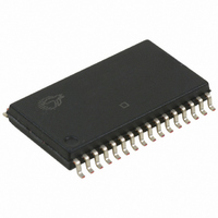
IC PROCESSOR NEURON 32-SOIC
Manufacturer
Cypress Semiconductor Corp
Series
Neuron®r
Datasheet
1.CY7C53150-20AXI.pdf
(16 pages)
Specifications of CY7C53120E2-10SXI
Package / Case
32-SOIC (11.30mm Width)
Applications
Network Processor
Core Processor
Pipelined
Program Memory Type
FLASH (2 kB), ROM (10 kB)
Controller Series
CY7C531xx
Ram Size
2K x 8
Interface
Serial
Number Of I /o
11
Voltage - Supply
4.5 V ~ 5.5 V
Operating Temperature
-40°C ~ 85°C
Mounting Type
Surface Mount
Product
Network Processor
Frequency
10 MHz
Supply Voltage (max)
2 V
Supply Voltage (min)
0.8 V
Supply Current (max)
55 mA
Maximum Operating Temperature
+ 85 C
Minimum Operating Temperature
- 40 C
Mounting Style
SMD/SMT
Core Operating Frequency
10MHz
Operating Supply Voltage (typ)
5V
Operating Supply Voltage (max)
5.5V
Operating Supply Voltage (min)
4.5V
Mounting
Surface Mount
Operating Temperature (max)
85C
Operating Temperature (min)
-40C
Operating Temperature Classification
Industrial
Core Size
8 Bit
No. Of I/o's
11
Program Memory Size
12KB
Ram Memory Size
2KB
Cpu Speed
10MHz
No. Of Timers
2
Digital Ic Case Style
QFP
Supply Voltage Range
4.5V To 5.5V
Rohs Compliant
Yes
Lead Free Status / RoHS Status
Lead free / RoHS Compliant
Lead Free Status / RoHS Status
Lead free / RoHS Compliant, Lead free / RoHS Compliant
Available stocks
Company
Part Number
Manufacturer
Quantity
Price
Company:

Part Number:
CY7C53120E2-10SXI
Manufacturer:
CYPRESS
Quantity:
2 290
Company:
Part Number:
CY7C53120E2-10SXI
Manufacturer:
CYPRESS
Quantity:
8
Part Number:
CY7C53120E2-10SXI
Manufacturer:
CYPRESS/赛普拉斯
Quantity:
20 000


Pin Descriptions
Document #: 38-10001 Rev. *G
Pin Name
CLK1
CLK2
RESET
SERVICE
IO0–IO3
IO4–IO7
IO8–IO10
D0–D7
R/W
E
A0–A15
V
V
Vpp
CP0–CP4 Communication
NC
DD
SS
Configurable
Configurable
I/O (Built-In
I/O (Built-In
I/O (Built-In
Pull ups)
Interface
Network
Pull up)
Pull up)
Output
Output
Output
Output
Input
Input
Input
Input
I/O
I/O
I/O
I/O
—
Oscillator connection or external clock
input.
Oscillator connection. Leave open when
external clock is input to CLK1. Maximum
of one external load.
Reset pin (active LOW). Note The
allowable external capacitance connected
to the RESET pin is 100–1000 pF.
Service pin (active LOW). Alternates
between input and output at a 76-Hz rate.
Large current-sink capacity (20 mA).
General I/O port. The output of timer/
counter 1 may be routed to IO0. The output
of Timer/Counter 2 may be routed to IO1.
General I/O port. The input to
Timer/Counter 1 may be derived from one
of IO4–IO7. The input to Timer/Counter 2
may be derived from IO4.
General I/O port. May be used for serial
communication under firmware control.
Bidirectional memory data bus.
Read/write control output for external
memory.
Enable clock control output for external
memory.
Memory address output port.
Power input (5V nom). All V
be connected together externally.
Power input (0V, GND). All V
be connected together externally.
In-circuit test mode control. If Vpp is high
when RESET is asserted, the I/O, address
and data buses become Hi-Z.
Bidirectional port supporting communi-
cations in three modes.
No connect. Must not be connected on the
user’s PC board, since they may be
connected internal to the chip.
Pin Function
DD
SS
pins must
pins must
TQFP-64 Pin No.
64, 63, 62, 61, 60,
59, 58, 57, 56, 55,
54, 53, 52, 51, 50,
28, 29, 30, 31, 32 19, 20, 17, 21, 22 20, 21, 18, 24, 25
1, 18, 27, 48, 49
8,19, 21, 25, 39 9, 13, 16, 23, 31
43, 42, 38, 37,
10, 11, 12, 13
36, 35, 34, 33
7, 20, 22, 26,
CY7C53150
14, 15, 16
40, 41, 44
2, 3, 4, 5
24
23
17
45
46
47
6
9
CY7C53150, CY7C53120
SOIC-32 Pin No.
CY7C53120xx
3, 30, 29, 28
27, 26, 24
18, 25, 32
2, 11, 12,
7, 6, 5, 4
N/A
N/A
N/A
N/A
N/A
15
14
10
1
8
TQFP-44 Pin No.
22, 23, 28, 33, 34,
7,13, 16, 26, 37
1, 6, 11, 12, 17,
CY7C53120xx
42, 36, 35, 32
31, 30, 27
29, 38, 41
4, 3, 2, 43
9, 10, 19,
39, 44
N/A
N/A
N/A
N/A
15
14
40
5
8
Page 5 of 16
[+] Feedback
Related parts for CY7C53120E2-10SXI
Image
Part Number
Description
Manufacturer
Datasheet
Request
R

Part Number:
Description:
Manufacturer:
Cypress Semiconductor Corp
Datasheet:
Part Number:
Description:
Manufacturer:
Cypress Semiconductor Corp
Datasheet:
Part Number:
Description:
Manufacturer:
Cypress Semiconductor Corp
Datasheet:
Part Number:
Description:
Manufacturer:
Cypress Semiconductor Corp
Datasheet:
Part Number:
Description:
Manufacturer:
Cypress Semiconductor Corp
Datasheet: