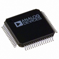
ADE7166ASTZF8 Analog Devices Inc, ADE7166ASTZF8 Datasheet - Page 106

ADE7166ASTZF8
Manufacturer Part Number
ADE7166ASTZF8
Description
IC ENERGY METER 1PHASE 64LQFP
Manufacturer
Analog Devices Inc
Specifications of ADE7166ASTZF8
Applications
Energy Measurement
Core Processor
8052
Program Memory Type
FLASH (8 kB)
Controller Series
ADE71xx
Ram Size
512 x 8
Interface
I²C, SPI, UART
Number Of I /o
20
Voltage - Supply
3.135 V ~ 3.465 V
Operating Temperature
-40°C ~ 85°C
Mounting Type
Surface Mount
Package / Case
64-LQFP
Ic Function
Single Phase Energy Measurement IC
Supply Voltage Range
3.13V To 3.46V, 2.4V To 3.7V
Operating Temperature Range
-40°C To +85°C
Digital Ic Case Style
LQFP
No. Of Pins
64
Lead Free Status / RoHS Status
Lead free / RoHS Compliant
Available stocks
Company
Part Number
Manufacturer
Quantity
Price
Company:
Part Number:
ADE7166ASTZF8
Manufacturer:
Analog Devices Inc
Quantity:
10 000
Company:
Part Number:
ADE7166ASTZF8-RL
Manufacturer:
Analog Devices Inc
Quantity:
10 000
ADE7116/ADE7156/ADE7166/ADE7169/ADE7566/ADE7569
LCD EXTERNAL CIRCUITRY
The voltage generation selection is made by the EXTRES bit (Bit
6) in the LCD configuration X SFR (LCDCONX, Address 0x9C).
This bit is cleared by default for charge pump voltage generation,
but it can be set to enable an external resistor ladder.
Charge Pump
Voltage generation through the charge pump requires external
capacitors to store charge. (Note that this feature is not available
in the ADE7116 or ADE7156.) The external connections to
LCDVA, LCDVB, and LCDVC, as well as to LCDVP1 and
LCDVP2, are shown in Figure 90.
External Resistor Ladder
To enable the external resistor ladder option, set the EXTRES
bit (Bit 6) in the LCD Configuration X SFR (LCDCONX,
Address 0x9C). When EXTRES = 1, the LCD waveform voltages
are supplied by the external resistor ladder. Because the LCD
voltages are not generated on-chip, the LCD bias compensation
implemented to maintain contrast over temperature and supply
is not possible.
The external circuitry needed for the resistor ladder option is
shown in Figure 92. The resistors required should be in the
range of 10 kΩ to 100 kΩ and should be based on the current
required by the LCD being used.
LCD WAVEFORM
CHARGE PUMP
Figure 91. External Circuitry for External Resistor Ladder Option:
Figure 92. External Circuitry for External Resistor Ladder Option:
CIRCUITRY
AND
Figure 90. External Circuitry for Charge Pump Option
LCD WAVEFORM
LCD WAVEFORM
CIRCUITRY
CIRCUITRY
LCDVP1
LCDVP2
LCDVC
LCDVB
LCDVA
1/2 Bias Configuration
1/3 Bias Configuration
100nF
LCDVP1
LCDVP2
LCDVP1
LCDVP2
LCDVC
LCDVB
LCDVA
LCDVC
LCDVB
LCDVA
470nF
470nF
470nF
Rev. B | Page 106 of 152
LCD FUNCTION IN PSM2 MODE
The LCDPSM2 (Bit 4) and LCDEN (Bit 7) in the LCD config-
uration SFR (LCDCON, Address 0x95) control the LCD
functionality in the PSM2 operating mode (see Table 100).
Note that the internal voltage reference must be enabled by setting
REF_BAT_EN bit (Bit 3) in the peripheral configuration SFR
(PERIPH, Address 0xF4) to allow LCD operation in PSM2 mode
(see Table 20).
Table 100. Bits Controlling LCD Functionality in PSM2
Mode
LCDPSM2
0
0
1
In addition, note that the LCD configuration and data memory
is retained when the display is turned off.
Example LCD Setup
An example of how to set up the LCD peripheral for a specific
LCD is described in this section with the following parameters:
•
•
•
A 96-segment LCD with 4× multiplexing requires 96/4 = 24
segment lines. Sixteen pins, FP0 to FP15, are automatically
dedicated for use as LCD segments. Eight more pins must be
chosen for the LCD function. Because the LCD has 4× multi-
plexing, all four common lines are used. As a result, COM2/FP28
and COM3/FP27 cannot be used as segment lines. Based on the
alternate functions of the pins used for FP16 through FP25,
FP16 to FP23 are chosen for the eight remaining segment lines.
These pins are enabled for LCD functionality in the LCD
segment enable SFR (LCDSEGE, Address 0x97) and LCD
Segment Enable 2 SFR (LCDSEGE2, Address 0xED).
To determine contrast setting for this 5 V LCD, Table 90 shows
the BIASLVL[5:0] setting in the LCD Configuration X SFR
(LCDCONX, Address 0x9C) that corresponds to a VC of 5 V in
1/3 bias mode. The maximum bias level setting for this LCD is
BIASLVL[5:0] = 101110.
Type of LCD: 5 V, 4× multiplexed with 1/3 bias, 96 segment
Voltage generation: internal charge pump
Refresh rate: 64 Hz
LCDEN
0
1
X
The display is off in PSM2.
Result
The display is off in PSM2.
The display is on in PSM2.


