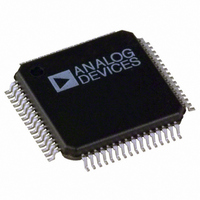
ADE7166ASTZF8 Analog Devices Inc, ADE7166ASTZF8 Datasheet - Page 140

ADE7166ASTZF8
Manufacturer Part Number
ADE7166ASTZF8
Description
IC ENERGY METER 1PHASE 64LQFP
Manufacturer
Analog Devices Inc
Specifications of ADE7166ASTZF8
Applications
Energy Measurement
Core Processor
8052
Program Memory Type
FLASH (8 kB)
Controller Series
ADE71xx
Ram Size
512 x 8
Interface
I²C, SPI, UART
Number Of I /o
20
Voltage - Supply
3.135 V ~ 3.465 V
Operating Temperature
-40°C ~ 85°C
Mounting Type
Surface Mount
Package / Case
64-LQFP
Ic Function
Single Phase Energy Measurement IC
Supply Voltage Range
3.13V To 3.46V, 2.4V To 3.7V
Operating Temperature Range
-40°C To +85°C
Digital Ic Case Style
LQFP
No. Of Pins
64
Lead Free Status / RoHS Status
Lead free / RoHS Compliant
Available stocks
Company
Part Number
Manufacturer
Quantity
Price
Company:
Part Number:
ADE7166ASTZF8
Manufacturer:
Analog Devices Inc
Quantity:
10 000
Company:
Part Number:
ADE7166ASTZF8-RL
Manufacturer:
Analog Devices Inc
Quantity:
10 000
ADE7116/ADE7156/ADE7166/ADE7169/ADE7566/ADE7569
Table 154. I
Bit
7
6
5
4
[3:2]
1
0
READ AND WRITE OPERATIONS
Figure 113 and Figure 114 depict I
respectively. Note that the LSB of the I2CADR SFR is used to
select whether a read or write operation is performed on the
slave device. During the read operation, the master acknowledges
are generated automatically by the I
generated NACK (no acknowledge) before the end of a read
operation is also automatically generated after the I2CRCT bits
have been read from the slave. If the I2CADR register is
updated during a transmission, instead of generating a stop at
the end of the read or write operation, the master generates a
start condition and continues with the next communication.
SDATA
SCLK
START BY
MASTER
Mnemonic
I2CBUSY
I2CNOACK
I2CRxIRQ
I2CTxIRQ
I2CFIFOSTAT
I2CACC_ERR
I2CTxWR_ERR
A6
2
1
C Interrupt Status Register SFR (SPI2CSTAT, Address 0xEA)
SERIAL BUS ADDRESS BYTE
A5
SDATA
SCLK
A4
START BY
MASTER
FRAME 1
A3
A2
Default
0
0
0
0
0
0
0
A6
1
A1
2
C read and write operations,
A5
SERIAL BUS ADDRESS BYTE
2
C peripheral. The master
A0
A4
Description
This bit is set to Logic 1 when the I
I
does not send an acknowledgement. The I
Write a 0 to this bit to clear it.
I
Write a 0 to this bit to clear it.
I
Write a 0 to this bit to clear it.
Status bits for 3- or 4-bytes deep I
used in I
I2CFIFOSTAT
00
01
10
11
Set when trying to write and read at the same time. Write a 0 to this bit to clear it.
Set when a write was attempted when the I
R/W
2
2
2
C no acknowledgement transmit interrupt. This bit is set to Logic 1 when the slave device
C receive interrupt. This bit is set to Logic 1 when the receive FIFO is not empty.
C Transmit Interrupt. This bit is set to Logic 1 when the transmit FIFO is empty.
ACK BY
SLAVE
FRAME 1
A3
9
A2
2
D7
C communication (receive or transmit) because only one FIFO is active at a time.
1
A1
D6
DATA BYTE 1 FROM MASTER
Figure 114. I
Figure 113. I
A0
D5
Rev. B | Page 140 of 152
R/W
D4
ACK BY
SLAVE
FRAME 2
Result
FIFO empty
Reserved
FIFO half full
FIFO full
D3
9
2
2
C Write Operation
C Read Operation
D2
D7
1
2
D1
D6
2
Reading the SPI/I
Address 0x9B)
Reading the SPI2CRx SFR should be done with a 2-cycle
instruction, such as
Mov a, spi2crx or Mov R0, spi2crx.
A 3-cycle instruction such as
Mov 3dh, spi2crx
does not transfer the right data into RAM Address 0x3D.
C FIFO. The FIFO monitored in these two bits is the one currently
C interface is used. When set, the Tx FIFO is emptied.
DATA BYTE 1 FROM MASTER
D0
D5
ACK BY
MASTER
2
9
D4
C communication is stopped after this event.
2
C transmit FIFO was full. Write a 0 to this bit to clear it.
FRAME 2
D3
D2
D7
1
2
C Receive Buffer SFR (SPI2CRx,
D6
D1
DATA BYTE N FROM SLAVE
D5
D0
ACK BY
SLAVE
D4
9
FRAME N + 1
D3
STOP BY
MASTER
D2
D1
D0
NACK BY
MASTER
9
STOP BY
MASTER


