CY7C66113-PVC Cypress Semiconductor Corp, CY7C66113-PVC Datasheet - Page 40
CY7C66113-PVC
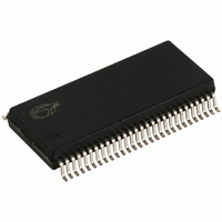
Manufacturer Part Number
CY7C66113-PVC
Description
IC MCU 8K USB HUB 4 PORT 56TSSOP
Manufacturer
Cypress Semiconductor Corp
Specifications of CY7C66113-PVC
Applications
USB Hub/Microcontroller
Core Processor
M8
Program Memory Type
OTP (8 kB)
Controller Series
USB Hub
Ram Size
256 x 8
Interface
I²C, USB, HAPI
Number Of I /o
31
Voltage - Supply
4 V ~ 5.5 V
Operating Temperature
0°C ~ 70°C
Mounting Type
Surface Mount
Package / Case
56-SSOP
Operating Temperature (max)
70C
Operating Temperature (min)
0C
Operating Temperature Classification
Commercial
Mounting
Surface Mount
Pin Count
56
Lead Free Status / RoHS Status
Contains lead / RoHS non-compliant
For Use With
CY3649 - PROGRAMMER HI-LO USB M8428-1339 - KIT LOW SPEED PERSONALITY BOARD
Lead Free Status / RoHS Status
Not Compliant, Contains lead / RoHS non-compliant
Other names
428-1330
Available stocks
Company
Part Number
Manufacturer
Quantity
Price
Company:

Part Number:
CY7C66113-PVC
Manufacturer:
CY
Quantity:
10


Table 19-1. Memory Allocation for Endpoints
When the SIE writes data to a FIFO, the internal data bus is driven by the SIE; not the CPU. This causes a short delay in the
CPU operation. The delay is three clock cycles per byte. For example, an 8-byte data write by the SIE to the FIFO generates a
delay of 2 s (3 cycles/byte * 83.33 ns/cycle * 8 bytes).
19.3
All USB devices are required to have a control endpoint 0 (EPA0 and EPB0) that is used to initialize and control each USB
address. Endpoint 0 provides access to the device configuration information and allows generic USB status and control accesses.
Endpoint 0 is bidirectional to both receive and transmit data. The other endpoints are unidirectional, but selectable by the user
as IN or OUT endpoints.
The endpoint mode registers are cleared during reset. When USB Status And Control Register Bits [6,7] are set to [0,0] or [1,0],
the endpoint zero EPA0 and EPB0 mode registers use the format shown in Figure 19-2.
USB Device Endpoint Zero Mode (A0, B0)
Bits[3..0] : Mode
Bit 4 : ACK
Bit 5: Endpoint 0 OUT Received
Bit 6: Endpoint 0 IN Received
Bit 7: Endpoint 0 SETUP Received
Document #: 38-08024 Rev. *A
Endpoints) & B (2 Endpoints)
Bit #
Bit Name
Read/Write
Reset
Label
EPB1
EPB0
EPA2
EPA1
EPA0
Two USB Addresses: A (3
These sets the mode which control how the control endpoint responds to traffic.
This bit is set whenever the SIE engages in a transaction to the register’s endpoint that completes with an ACK packet.
1 = Token received is an OUT token. 0 = Token received is not an OUT token. This bit is set by the SIE to report the type
of token received by the corresponding device address is an OUT token. The bit must be cleared by firmware as part of
the USB processing.
1 = Token received is an IN token. 0 = Token received is not an IN token. This bit is set by the SIE to report the type of
token received by the corresponding device address is an IN token. The bit must be cleared by firmware as part of the USB
processing.
1 = Token received is a SETUP token. 0 = Token received is not a SETUP token. This bit is set ONLY by the SIE to report
the type of token received by the corresponding device address is a SETUP token. Any write to this bit by the CPU will
clear it (set it to 0). The bit is forced HIGH from the start of the data packet phase of the SETUP transaction until the start
of the ACK packet returned by the SIE. The CPU should not clear this bit during this interval, and subsequently, until the
CPU first does an IORD to this endpoint 0 mode register. The bit must be cleared by firmware as part of the USB processing.
Note: In 5-endpoint mode (USB Status And Control Register Bits [7,6] are set to [0,1] or [1,1]), Register 0x42 serves as
non-control endpoint 3, and has the format for non-control endpoints shown in Figure 19-3.
USB Control Endpoint Mode Registers
Address
0xD8
Start
0xE0
0xE8
0xF0
0xF8
[0,0]
7
Endpoint 0
SETUP Received
R/W
0
Size
8
8
8
8
8
6
Endpoint 0 IN
Received
R/W
0
Endpoints) &B (2 Endpoints)
Label
EPB0
EPB1
EPA0
EPA1
EPA2
Two USB Addresses: A (3
USB Status And Control Register (0x1F) Bits [7, 6]
Figure 19-2. USB Device Endpoint Zero Mode Registers
Address
5
Endpoint 0
OUT
Received
R/W
0
0xA8
0xB0
0xB8
0xC0
0xE0
Start
[1,0]
Size
32
32
8
8
8
4
ACK
R/W
0
Label
EPA1
EPA4
EPA3
EPA2
EPA0
One USB Address:
A (5 Endpoints)
3
Mode Bit 3
R/W
0
Address
0xD8
0xE0
0xE8
Start
0xF0
0xF8
[0,1]
2
Mode Bit 2
R/W
0
Size
8
8
8
8
8
ADDRESSES
Label
EPA3
EPA4
EPA0
EPA1
EPA2
1
Mode Bit 1
R/W
0
One USB Address:
A (5 Endpoints)
Address
CY7C66013
CY7C66113
0x12(A0) and 0x42(B0)
0xA8
0xB0
0xB8
0xC0
0xE0
Start
[1,1]
Page 40 of 58
0
Mode Bit 0
R/W
0
Size
32
32
8
8
8
Related parts for CY7C66113-PVC
Image
Part Number
Description
Manufacturer
Datasheet
Request
R

Part Number:
Description:
Manufacturer:
Cypress Semiconductor Corp
Datasheet:
Part Number:
Description:
Manufacturer:
Cypress Semiconductor Corp
Datasheet:
Part Number:
Description:
Manufacturer:
Cypress Semiconductor Corp
Datasheet:
Part Number:
Description:
Manufacturer:
Cypress Semiconductor Corp
Datasheet:
Part Number:
Description:
Manufacturer:
Cypress Semiconductor Corp
Datasheet: