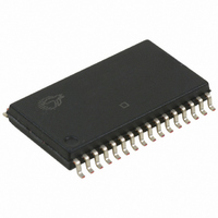
CY7C53120E2-10SXIT Cypress Semiconductor Corp, CY7C53120E2-10SXIT Datasheet - Page 7

CY7C53120E2-10SXIT
Manufacturer Part Number
CY7C53120E2-10SXIT
Description
IC PROCESSOR NEURON 32-SOIC
Manufacturer
Cypress Semiconductor Corp
Series
Neuron®r
Datasheet
1.CY7C53120E2-10SXIT.pdf
(14 pages)
Specifications of CY7C53120E2-10SXIT
Applications
Network Processor
Core Processor
Pipelined
Program Memory Type
FLASH (2 kB), ROM (10 kB)
Controller Series
CY7C531xx
Ram Size
2K x 8
Interface
Serial
Number Of I /o
11
Voltage - Supply
4.5 V ~ 5.5 V
Operating Temperature
-40°C ~ 85°C
Mounting Type
Surface Mount
Package / Case
32-SOIC (11.30mm Width)
Lead Free Status / RoHS Status
Lead free / RoHS Compliant
Document #: 38-10001 Rev. *E
Electrical Characteristics
LVI Trip Point (V
Notes
11. Standard outputs are IO4–IO10, CP0, CP1, and CP4. (RESET is an open drain input/output. CLK2 must have < 15 pF load.) For CY7C53150, standard outputs
12. IO4–IO7 and SERVICE have configurable pull ups. RESET has a permanent pull up.
13. Supply current measurement conditions: V
14. Supported through an external oscillator only.
Parameter
V
V
V
V
V
I
I
I
I
CY7C53120E2, CY7C53120E4, and CY7C53150
in
pu
DD
DDsleep
IL
IH
OL
OH
hys
also include A0–A15, D0–D7, E, and R/W.
oscillator clock input, differential receiver disabled. The differential receiver adds approximately 200 µA typical and 600 µA maximum when enabled. It is enabled
on either of the following conditions:
• Neuron chip in Operating mode and Comm Port in Differential mode.
• Neuron chip in Sleep mode and Comm Port in Differential mode and Comm Port Wake-up not masked.
Input Low Voltage
Input High Voltage
Low-Level Output Voltage
High-Level Output Voltage
Hysteresis (Excluding CLK1)
Input Current (Excluding Pull Ups) (V
Pull Up Source Current (V
Operating Mode Supply Current
20-MHz Clock
10-MHz Clock
5-MHz Clock
2.5-MHz Clock
1.25-MHz Clock
0.625-MHz Clock
Sleep Mode Supply Current
IO0–IO10, CP0, CP3, CP4, SERVICE, D0-D7, RESET
CP0, CP1 (Differential)
IO0–IO10, CP0, CP3, CP4, SERVICE, D0-D7, RESET
CP0, CP1 (Differential)
I
Standard Outputs (I
High Sink (IO0–IO3), SERVICE, RESET (I
High Sink (IO0–IO3), SERVICE, RESET (I
Maximum Sink (CP2, CP3) (I
Maximum Sink (CP2, CP3) (I
I
Standard Outputs (I
High Sink (IO0 – IO3), SERVICE (I
Maximum Source (CP2, CP3) (I
Maximum Source (CP2, CP3) (I
out
out
< 20 μA
< 20 μA
DD
)
Part Number
[14]
(V
DD
OL
OH
DD
Description
= 1.4 mA)
= 5V, all outputs under no-load conditions, all inputs < 0.2V or > (V
= 4.5V–5.5V)
= –1.4 mA)
out
[1, 13]
= 0 V, Output = High-Z)
OL
OL
[13]
OH
OH
= 40 mA)
= 15 mA)
[11]
40-MHz Clock
[11]
OH
SS
= –40 mA)
= –15 mA)
to V
= –1.4 mA)
DD
OL
OL
)
= 20 mA)
= 10 mA)
[12]
[14]
[12]
Programmable
V
V
V
V
V
Min.
3.8
DD
DD
DD
DD
DD
Min.
175
2.0
60
—
—
—
—
—
—
—
—
—
—
—
—
—
—
—
—
—
– 0.1
– 0.4
– 0.4
– 1.0
– 0.4
DD
Typ.
– 0.2V), configurable pull ups off, crystal
Typ.
4.1
—
—
—
—
—
—
—
—
—
—
—
—
—
—
—
—
—
—
—
—
—
—
—
—
—
—
Programmable
CY7C53150
CY7C53120
Max.
±10
260
100
Max.
0.8
0.1
0.4
0.8
0.4
1.0
0.4
55
32
20
12
—
—
—
—
—
—
—
—
4.4
8
7
3
Page 7 of 14
Unit
Unit
mV
mA
μA
μA
μA
V
V
V
V
V
[+] Feedback


