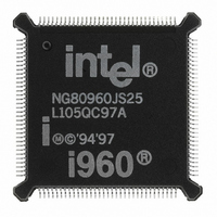
NG80960JS25 Intel, NG80960JS25 Datasheet - Page 22

NG80960JS25
Manufacturer Part Number
NG80960JS25
Description
IC MPU I960JS 3V 25MHZ 132-QFP
Manufacturer
Intel
Datasheet
1.NG80960JS25.pdf
(86 pages)
Specifications of NG80960JS25
Rohs Status
RoHS non-compliant
Processor Type
i960
Features
JS suffix, 32-Bit, 16K Cache
Speed
25MHz
Voltage
3V
Mounting Type
Surface Mount
Package / Case
132-QFP
Other names
820348
Available stocks
Company
Part Number
Manufacturer
Quantity
Price
80960JA/JF/JD/JS/JC/JT 3.3 V Embedded 32-Bit Microprocessor
22
Table 9.
Table 10. Pin Description—Interrupt Unit Signals
Pin Description—Processor Control Signals, Test Signals, and Power (Sheet 2 of 2)
XINT[7:0]#
VCCPLL
TRST#
NAME
NAME
VCC5
NMI#
TDO
TMS
V
V
NC
CC
SS
A(E/L)
TYPE
TYPE
R(Q)
P(Q)
A(L)
S(L)
A(E)
HQ)
O
–
–
–
–
–
I
I
I
I
TEST DATA OUTPUT is the serial output pin for JTAG. TDO is driven on the falling
edge of TCK during the SHIFT-IR and SHIFT-DR states of the Test Access Port. At
other times, TDO floats. TDO does not float during ONCE mode.
TEST RESET asynchronously resets the Test Access Port (TAP) controller function
of IEEE 1149.1 Boundary Scan testing (JTAG). When using the Boundary Scan
feature, connect a pull-down resistor between this pin and V
used, this pin must be connected to V
Section 4.3, “Connection Recommendations” on page
TEST MODE SELECT is sampled at the rising edge of TCK to select the operation of
the test logic for IEEE 1149.1 Boundary Scan testing.
POWER pins intended for external connection to a V
PLL POWER is a separate V
is intended for external connection to the V
add a simple bypass filter circuit to reduce noise-induced clock jitter and its effects on
timing relationships.
5 V REFERENCE VOLTAGE input is the reference voltage for the 5 V-tolerant I/O
buffers. This signal should be connected to +5 V for use with inputs which exceed
3.3 V. When all inputs are from 3.3 V components, this pin should be connected to
3.3 V.
GROUND pins intended for external connection to a V
NO CONNECT pins. Do not make any system connections to these pins.
EXTERNAL INTERRUPT pins are used to request interrupt service. The XINT[7:0]#
pins may be configured in three modes:
Dedicated Mode: Each pin is assigned a dedicated interrupt level. Dedicated inputs
may be programmed to be level (low) or edge (falling) sensitive.
Expanded Mode: All eight pins act as a vectored interrupt source. The interrupt pins
are level sensitive in this mode.
Mixed Mode: The XINT[7:5]# pins act as dedicated sources and the XINT[4:0]# pins
act as the five most significant bits of a vectored source. The least significant bits of
the vectored source are set to 010
Unused external interrupt pins should be connected to V
NON-MASKABLE INTERRUPT causes a non-maskable interrupt event to occur.
NMI# is the highest priority interrupt source and is falling edge-triggered. when NMI#
is unused, it should be connected to V
CC
supply pin for the phase lock loop clock generator. It
2
DESCRIPTION
DESCRIPTION
internally.
SS
CC
; however, no resistor is required. See
.
CC
board plane. In noisy environments,
CC
SS
36.
board plane.
CC
board plane.
.
SS
. When TAP is not
Datasheet


