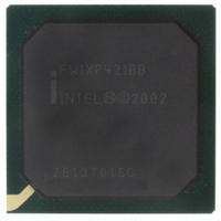
FWIXP421BB Intel, FWIXP421BB Datasheet - Page 111

FWIXP421BB
Manufacturer Part Number
FWIXP421BB
Description
IC NETWRK PROCESSR 266MHZ 492BGA
Manufacturer
Intel
Specifications of FWIXP421BB
Processor Type
Network
Features
XScale Core
Speed
266MHz
Voltage
1.3V
Mounting Type
Surface Mount
Package / Case
492-BGA
Core Operating Frequency
266MHz
Package Type
BGA
Pin Count
492
Mounting
Surface Mount
Operating Temperature (max)
70C
Operating Temperature (min)
0C
Operating Temperature Classification
Commercial
Lead Free Status / RoHS Status
Contains lead / RoHS non-compliant
Other names
852277
Available stocks
Company
Part Number
Manufacturer
Quantity
Price
Part Number:
FWIXP421BB
Manufacturer:
BGA
Quantity:
20 000
Intel
Table 60.
Table 61.
August 2006
Document Number: 252479-006US
®
IXP42X product line and IXC1100 control plane processors
HPI Timing Symbol Description
HPI-8 Mode Write Access Values
Notes:
1.
2.
3.
4.
5.
6.
7.
Notes:
1.
2.
3.
4.
5.
6.
7.
T
T
T
T
T
Symbol
cs2hds1val
hds1_pulse
data_setup
add_setup
data_hold
State
T
recov
T1
T2
T3
T4
T5
The address phase parameter (T1) must be set to a minimum value of 2. This value allows three T
clocks for the address phase. This setting is required to ensure that in the event of an HRDY, the
Intel
recognize the HRDY and hold the address phase for at least one clock pulse after the HRDY is de-
active.
The data setup phase parameter (T2) must be set to a minimum value of 2. This value allows three T
clocks for setup phase.
The data strobe phase parameter (T3) must be set to a minimum value of 1. This value allows two T
clocks for the data phase. This setting is required to ensure that in the event of an HRDY, the Intel
IXP42X Product Line and Intel
recognize the HRDY and hold the data setup phase for at least one clock pulse after the HRDY is de-
active.
Setting the recovery phase parameter (T5) will adjust the duration between successive accesses on
the Expansion Bus interface.
HRDY can be asserted by the DSP at any point in the access. The interface will not leave states T1 or
T3 until HRDY is de-active.
One cycle is the period of the Expansion Bus clock.
Timing tests were performed with a 70-pF capacitor to ground.
®
®
IXP42X Product Line and Intel
IXP42X Product Line and Intel
Valid time that address is asserted on the line. The
address is asserted at the same time as chip select.
Delay from chip select being active and the HDS1 data
strobe being active.
Pulse width of the HDS1 data strobe
Data valid prior to the rising edge of the HDS1 data
strobe.
Data valid after the rising edge of the HDS1 data strobe.
Time required between successive accesses on the
expansion interface.
Intel
Setup/Chip Select Timing
®
IXP42X Product Line of Network Processors and IXC1100 Control Plane Processor
Recovery Phase
Address Timing
Strobe Timing
Description
Hold Timing
®
®
Parameter
IXC1100 Control Plane processors has had sufficient time to
IXC1100 Control Plane processors has had sufficient time to
®
®
IXC1100 Control Plane processors has had sufficient time to
IXC1100 Control Plane processors has had sufficient time to
Min.
3
3
2
3
2
Max.
16
17
4
4
4
Min.
11
3
4
4
2
4
Cycles
Cycles
Cycles
Cycles
Cycles
Unit
Max.
45
36
17
4
5
5
Cycles
Cycles
Cycles
Cycles
Cycles
Cycles
Units
1, 5,
3, 5,
Notes
2,
Datasheet
6
6
6
1, 5,
2, 4,
3, 5,
Notes
6
6
5,
3,
4,
6
6
6
®
®
111
6
5
6


