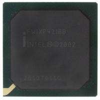
FWIXP421BB Intel, FWIXP421BB Datasheet - Page 91

FWIXP421BB
Manufacturer Part Number
FWIXP421BB
Description
IC NETWRK PROCESSR 266MHZ 492BGA
Manufacturer
Intel
Specifications of FWIXP421BB
Processor Type
Network
Features
XScale Core
Speed
266MHz
Voltage
1.3V
Mounting Type
Surface Mount
Package / Case
492-BGA
Core Operating Frequency
266MHz
Package Type
BGA
Pin Count
492
Mounting
Surface Mount
Operating Temperature (max)
70C
Operating Temperature (min)
0C
Operating Temperature Classification
Commercial
Lead Free Status / RoHS Status
Contains lead / RoHS non-compliant
Other names
852277
Available stocks
Company
Part Number
Manufacturer
Quantity
Price
Part Number:
FWIXP421BB
Manufacturer:
BGA
Quantity:
20 000
Intel
Figure 16.
Table 47.
August 2006
Document Number: 252479-006US
®
IXP42X product line and IXC1100 control plane processors
Note:
PCI Input Timing
PCI Bus Signal Timings
T
T
T
T
T
T
Notes:
1.
2.
3.
4.
5.
6.
7.
8.
Symbol
clk2outb
clk2out
setupb
setup
rst-off
hold
V
Input
See the timing measurement conditions.
Parts compliant to the 3.3 V signaling environment.
REQ# and GNT# are point-to-point signals and have different output valid delay and input setup
times than do bused signals. GNT# has a setup of 10 ns for 33 MHz and 5 ns for 66 MHz; REQ# has
a setup of 12 ns for 33 MHz and 5 ns for 66 MHz.
RST# is asserted and de-asserted asynchronously with respect to CLK.
All PCI outputs must be asynchronously driven to a tri-state value when RST# is active.
Setup time applies only when the device is not driving the pin. Devices cannot drive and receive
signals at the same time.
Timing was tested with a 70-pF capacitor to ground.
For additional information, see the PCI Local Bus Specification, Rev. 2.2.
HI
CLK
= 0.6 V
Clock to output for all bused
signals. This is the PCI_AD[31:0],
PCI_CBE_N [3:0], PCI_PAR,
PCI_FRAME_N, PCI_IRDY_N,
PCI_TRDY_N, PCI_STOP_N,
PCI_DEVSEL_N, PCI_PERR_N,
PCI_SERR_N
Clock to output for all point-to-
point signals. This is the
PCI_GNT_N and PCI_REQ_N(0)
only.
Input setup time for all bused
signals. This is the PCI_AD[31:0],
PCI_CBE_N [3:0], PCI_PAR,
PCI_FRAME_N, PCI_IRDY_N,
PCI_TRDY_N, PCI_STOP_N,
PCI_DEVSEL_N, PCI_PERR_N,
PCI_SERR_N
Input setup time for all point-to-
point signals. This is the
PCI_REQ_N and PCI_GNT_N(0)
only.
Input hold time from clock.
Reset active-to-output float delay
CC
and V
Parameter
Intel
LOW
®
IXP42X Product Line of Network Processors and IXC1100 Control Plane Processor
= 0.2 V
CC
10, 12
Min.
2
2
7
0
33 MHz
T
setup(b)
Max.
Inputs
Valid
11
12
40
T
hold
Min.
1
1
3
5
0
66 MHz
Max.
40
6
6
Units
ns
ns
ns
ns
ns
ns
A9573-01
Datasheet
1, 2, 5,
1, 2, 5,
4, 6, 7,
5, 6, 7,
4, 7,
4, 7,
Notes
7,
7,
8
8
8
8
8
8
91


