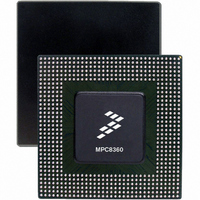
MPC8360VVALFH Freescale Semiconductor, MPC8360VVALFH Datasheet - Page 15

MPC8360VVALFH
Manufacturer Part Number
MPC8360VVALFH
Description
IC MPU PWRQUICC II 740-TBGA
Manufacturer
Freescale Semiconductor
Datasheet
1.MPC8360CZUAJDG.pdf
(108 pages)
Specifications of MPC8360VVALFH
Processor Type
MPC83xx PowerQUICC II Pro 32-Bit
Speed
667MHz
Voltage
1.3V
Mounting Type
Surface Mount
Package / Case
740-TBGA
For Use With
MPC8360EA-MDS-PB - KIT APPLICATION DEV 8360 SYSTEMMPC8360E-RDK - BOARD REFERENCE DESIGN FOR MPC
Lead Free Status / RoHS Status
Lead free / RoHS Compliant
Features
-
Available stocks
Company
Part Number
Manufacturer
Quantity
Price
Company:
Part Number:
MPC8360VVALFH
Manufacturer:
Freescale Semiconductor
Quantity:
10 000
Company:
Part Number:
MPC8360VVALFHA
Manufacturer:
Freescale Semiconductor
Quantity:
10 000
Part Number:
MPC8360VVALFHA
Manufacturer:
FREESCALE
Quantity:
20 000
Table 6
4
This section provides the clock input DC and AC electrical characteristics for the MPC8360E/58E.
Freescale Semiconductor
DDR I/O
65% utilization
R
R
2 pairs of clocks
Local Bus I/O
Load = 25 pf
3 pairs of clocks
PCI I/O
Load = 30 pF
10/100/1000
Ethernet I/O
Load = 20 pF
Other I/O
s
t
MPC8360E/MPC8358E PowerQUICC II Pro Processor Revision 2.x TBGA Silicon Hardware Specifications, Rev. 4
= 50 Ω
= 20 Ω
Interface
Clock Input Timing
shows the estimated typical I/O power dissipation for the device.
The rise/fall time on QUICC Engine block input pins should not exceed 5
ns. This should be enforced especially on clock signals. Rise time refers to
signal transitions from 10% to 90% of V
from 90% to 10% of V
200 MHz, 1 × 32 bits
200 MHz, 1 × 64 bits
200 MHz, 2 × 32 bits
266 MHz, 1 × 32 bits
266 MHz, 1 × 64 bits
266 MHz, 2 × 32 bits
333 MHz, 1 × 32 bits
333 MHz, 1 × 64 bits
333 MHz, 2 × 32 bits
133 MHz, 32 bits
83 MHz, 32 bits
66 MHz, 32 bits
50 MHz, 32 bits
33 MHz, 32 bits
66 MHz, 32 bits
MII or RMII
GMII or TBI
RGMII or RTBI
—
Parameter
Table 6. Estimated Typical I/O Power Dissipation
DD
(1.8 V)
GV
0.35
0.46
0.53
0.81
0.3
0.4
0.6
0.7
0.4
.
—
—
—
—
—
—
—
—
—
—
DD
(2.5 V)
GV
NOTE
0.46
0.58
0.92
0.56
1.11
0.65
0.82
0.7
1.3
—
—
—
—
—
—
—
—
—
—
DD
DD
(3.3 V)
OV
0.22
0.14
0.12
0.09
0.05
0.07
; fall time refers to transitions
0.1
—
—
—
—
—
—
—
—
—
—
—
—
DD
(3.3 V)
LV
0.01
0.04
—
—
—
—
—
—
—
—
—
—
—
—
—
—
—
—
—
DD
(2.5 V)
LV
0.04
—
—
—
—
—
—
—
—
—
—
—
—
—
—
—
—
—
—
DD
Unit
W
W
W
W
W
W
W
W
W
W
W
W
W
W
W
W
W
W
W
Multiply by
number of
interfaces used.
Clock Input Timing
Comments
—
—
—
—
—
—
—
—
—
—
—
—
—
—
—
—
15


