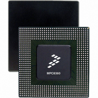
MPC8360VVALFH Freescale Semiconductor, MPC8360VVALFH Datasheet - Page 77

MPC8360VVALFH
Manufacturer Part Number
MPC8360VVALFH
Description
IC MPU PWRQUICC II 740-TBGA
Manufacturer
Freescale Semiconductor
Datasheet
1.MPC8360CZUAJDG.pdf
(108 pages)
Specifications of MPC8360VVALFH
Processor Type
MPC83xx PowerQUICC II Pro 32-Bit
Speed
667MHz
Voltage
1.3V
Mounting Type
Surface Mount
Package / Case
740-TBGA
For Use With
MPC8360EA-MDS-PB - KIT APPLICATION DEV 8360 SYSTEMMPC8360E-RDK - BOARD REFERENCE DESIGN FOR MPC
Lead Free Status / RoHS Status
Lead free / RoHS Compliant
Features
-
Available stocks
Company
Part Number
Manufacturer
Quantity
Price
Company:
Part Number:
MPC8360VVALFH
Manufacturer:
Freescale Semiconductor
Quantity:
10 000
Company:
Part Number:
MPC8360VVALFHA
Manufacturer:
Freescale Semiconductor
Quantity:
10 000
Part Number:
MPC8360VVALFHA
Manufacturer:
FREESCALE
Quantity:
20 000
Table 67
Freescale Semiconductor
NC
Notes:
1. This pin is an open drain signal. A weak pull-up resistor (1 kΩ) should be placed on this pin to OV
2. This pin is an open drain signal. A weak pull-up resistor (2–10 kΩ) should be placed on this pin to OV
3. This output is actively driven during reset rather than being three-stated during reset.
4. These JTAG pins have weak internal pull-up P-FETs that are always enabled.
5. This pin should have a weak pull up if the chip is in PCI host mode. Follow PCI specifications recommendation.
6. These are On Die Termination pins, used to control DDR2 memories internal termination resistance
7. This pin must always be tied to GND.
8. This pin must always be left not connected.
9. Refers to MPC8360E PowerQUICC II Pro Integrated Communications Processor Family Reference Manual section on
10. It is recommended that MDIC0 be tied to GND using an 18.2 Ω resistor and MDIC1 be tied to DDR power using an 18.2 Ω
MEMC1_MDQ[0:63]
MEMC_MECC[0:4]/MSRCID[0:4]
MEMC_MECC[5]/MDVAL
MEMC_MECC[6:7]
MEMC_MDM[0:8]
MEMC_MDQS[0:8]
MEMC_MBA[0:1]
MEMC_MBA[2]
MEMC_MA[0:14]
“RGMII Pins,” for information about the two UCC2 Ethernet interface options.
resistor for DDR2.
MPC8360E/MPC8358E PowerQUICC II Pro Processor Revision 2.x TBGA Silicon Hardware Specifications, Rev. 4
shows the pin list of the MPC8358E TBGA package.
Signal
Signal
Table 66. MPC8360E TBGA Pinout Listing (continued)
Table 67. MPC8358E TBGA Pinout Listing
AM20, AU19
AJ34, AK33, AL33, AL35, AJ33, AK34, AK32,
AM36, AN37, AN35, AR34, AT34, AP37, AP36,
AR36, AT35, AP34, AR32, AP32, AM31, AN33,
AM34, AM33, AM30, AP31, AM27, AR30, AT32,
AN29, AP29, AN27, AR29, AN8, AN7, AM8, AM6,
AP9, AN9, AT7, AP7, AU6, AP6, AR4, AR3, AT6,
AT5, AR5, AT3, AP4, AM5, AP3, AN3, AN5, AL5,
AN4, AM2, AL2, AH5, AK3, AJ2, AJ3, AH4, AK4,
AH3
AP24, AN22, AM19, AN19, AM24
AM23
AM22, AN18
AL36, AN34, AP33, AN28,AT9, AU4, AM3,
AJ6,AP27
AK35, AP35, AN31, AM26,AT8, AU3, AL4, AJ5,
AP26
AU29, AU30
AT30
AU21, AP22, AP21, AT21, AU25, AU26, AT23,
AR26, AU24, AR23, AR28, AU23, AR22, AU20,
AR18
DDR SDRAM Memory Controller Interface
Package Pin Number
Package Pin Number
No Connect
Pin Type
Pin Type
I/O
I/O
I/O
I/O
I/O
—
O
O
O
O
DD
Package and Pin Listings
DD
.
Supply
Supply
Power
Power
GV
GV
GV
GV
GV
GV
GV
GV
GV
—
DD
DD
DD
DD
DD
DD
DD
DD
DD
Notes
Notes
—
—
—
—
—
—
—
—
—
77


