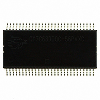
CY7C68300C-56PVXC Cypress Semiconductor Corp, CY7C68300C-56PVXC Datasheet - Page 10

CY7C68300C-56PVXC
Manufacturer Part Number
CY7C68300C-56PVXC
Description
IC USB 2.0 BRIDGE AT2LP 56-SSOP
Manufacturer
Cypress Semiconductor Corp
Series
CY7Cr
Type
USB to ATA/ATAPI Bridger
Datasheets
1.CY7C68300C-56PVXC.pdf
(42 pages)
2.CY7C68320C-100AXA.pdf
(44 pages)
3.CY7C68300C-56PVXC.pdf
(42 pages)
Specifications of CY7C68300C-56PVXC
Package / Case
56-SSOP
Controller Type
USB 2.0 Controller
Interface
I²C
Voltage - Supply
3.15 V ~ 3.45 V
Current - Supply
50mA
Operating Temperature
0°C ~ 70°C
Mounting Type
Surface Mount
Maximum Operating Temperature
+ 70 C
Minimum Operating Temperature
0 C
Mounting Style
SMD/SMT
Number Of Bits
48
Operating Temperature Range
0 C to + 70 C
Supply Current
10 mA
Operating Supply Voltage
3.3 V
Controller Family/series
(8051) USB
Core Size
8 Bit
No. Of I/o's
6
Embedded Interface Type
I2C, USB
Digital Ic Case Style
SSOP
Supply Voltage Range
3V To 3.6V
Rohs Compliant
Yes
Operating Temperature (min)
0C
Operating Temperature Classification
Commercial
Operating Temperature (max)
70C
Package Type
SSOP
Rad Hardened
No
Lead Free Status / RoHS Status
Lead free / RoHS Compliant
For Use With
CY4615B - KIT USB TO ATA REFERENCE DESIGN
Lead Free Status / Rohs Status
Lead free / RoHS Compliant
Other names
428-2266-5
CY7C68300C-56PVXC
CY7C68300C-56PVXC
Available stocks
Company
Part Number
Manufacturer
Quantity
Price
Company:
Part Number:
CY7C68300C-56PVXC
Manufacturer:
HITACHI
Quantity:
2 000
Company:
Part Number:
CY7C68300C-56PVXC
Manufacturer:
CY
Quantity:
8
Part Number:
CY7C68300C-56PVXC
Manufacturer:
CYPRESS/赛普拉斯
Quantity:
20 000
Pin Descriptions
The following table lists the pinouts for the 56-pin SSOP, 56-pin QFN, and 100-pin TQFP package options for the AT2LP. Refer to the
Pin Diagrams
on the CY7C68300A pinout, refer to the CY7C68300A data sheet that is found in the ’EZ-USB AT2’ folder of the CY4615C Reference
Design Kit CD.
Table 1. AT2LP Pin Descriptions
Note Italic pin names denote pin functionality during CY7C68300A compatibility mode
Document 001-05809 Rev. *E
Notes
1. If byte 8, bit 4 of the EEPROM is set to ‘0’, the ATA interface pins are only active when VBUS_ATA_EN is asserted. See
2. A ‘#’ sign after the pin name indicates that it is active LOW.
3. The General Purpose inputs can be enabled on ATAPUEN, PWR500#, and DRVPWRVLD via EEPROM byte 8, bit 7 on CY7C68320C/CY7C68321C.
TQFP
26
100
10
12
13
14
15
16
17
18
19
20
21
22
23
24
25
27
28
11
1
2
3
4
5
6
7
8
9
[3]
QFN
13
N/A
N/A
N/A
N/A
N/A
56
55
56
10
11
12
14
1
2
3
4
5
6
7
8
9
[3]
on page 5 for differences between the 68300C/01C and 68320C/321C pinouts for the 56-pin packages. For information
SSOP
N/A
N/A
N/A
N/A
N/A
56
10
11
12
13
14
15
16
17
18
19
20
21
6
7
8
9
GND (RESERVED)
PWR500#
Pin Name
XTALOUT
(PU 10K)
DMINUS
DMARQ
SYSIRQ
XTALIN
DPLUS
IORDY
AGND
AV
GND
GND
GND
GND
GND
V
V
V
NC
NC
CC
CC
CC
CC
[2]
PWR
PWR
PWR
PWR
Type
GND
GND
GND
GND
GND
Xtal
Xtal
Pin
I/O
I/O
I
I
O
[1]
[1]
I
Default State
at Startup
High-Z
High-Z
Input
Input
Input
Xtal
Xtal
V
Ground.
ATA control. Apply a 1k pull up to 3.3V.
ATA control.
Ground.
Analog V
possible.
24 MHz crystal output. (See
13).
24 MHz crystal input. (See
13).
Analog ground. Connect to ground with as short a path as
possible.
No connect.
V
USB D+ signal (See
USB D–signal (See
Ground.
V
Ground.
USB interrupt request. (See
HIGH. Connect to GND if functionality is not used.
Ground.
bMaxPower request granted indicator. (See
on page 15). Active LOW.
N/A for CY7C68320C/CY7C68321C 56-pin packages.
Reserved. Tie to GND.
No connect.
CC
CC
CC
. Connect to 3.3V power source.
. Connect to 3.3V power source.
. Connect to 3.3V power source.
CC
. Connect to V
CY7C68300C, CY7C68301C
CY7C68320C, CY7C68321C
Pin Description
DPLUS, DMINUS
DPLUS, DMINUS
VBUS_ATA_ENABLE
CC
XTALIN, XTALOUT
SYSIRQ
XTALIN, XTALOUT
through the shortest path
on page 14). Active
on page 13).
on page 13).
on page 15.
Page 10 of 42
PWR500#
on page
on page
[+] Feedback


