PKM4113DPINB Ericsson Power Modules, PKM4113DPINB Datasheet - Page 11
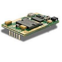
PKM4113DPINB
Manufacturer Part Number
PKM4113DPINB
Description
DC/DC Converters & Regulators 12 Vdc 11A Iso Input 36-75V 132W
Manufacturer
Ericsson Power Modules
Series
PKM-Dr
Datasheet
1.PKM4113DPINB.pdf
(29 pages)
Specifications of PKM4113DPINB
Product
Isolated
Output Power
30 W
Input Voltage Range
36 V to 75 V
Number Of Outputs
1
Output Voltage (channel 1)
1.5 V
Output Current (channel 1)
20 A
Isolation Voltage
1.5 KV
Package / Case Size
Quarter Brick
Output Type
Isolated
Lead Free Status / Rohs Status
Lead free / RoHS Compliant
Available stocks
Company
Part Number
Manufacturer
Quantity
Price

Part Number:
PKM4113DPINB
Manufacturer:
ERICSSON/爱立信
Quantity:
20 000


E
5.0V, 25A /125W Typical Characteristics
Start-up
Start-up enabled by connecting V
T
I
Output Ripple & Noise
Output voltage ripple at:
T
I
Output Voltage Adjust (see operating information)
Passive adjust
The resistor value for an adjusted output voltage is calculated by
using the following equations:
Output Voltage Adjust Upwards, Increase:
Example: Increase 4% =>V
Output Voltage Adjust Downwards, Increase:
Example: Decrease 2% =>V
kΩ = 404.32 kΩ
Prepared (also subject responsible if other)
EQUENXU
Approved
SEC/D (Julia You)
PKM 4000D PINB series
DC/DC converters, Input 36-75 V, Output up to 35 A/132 W
O
O
⎛
⎜ ⎜
⎝
. 5
Radj
Radj
P1
P1
= 25 A resistive load.
= 25 A resistive load.
. 5
11
= +25°C, V
= +25°C, V
11
⎛
⎜ ⎜
⎝
=
=
100
. 1
×
2
⎛
⎜ ⎜
⎝
. 5
5
225
. 5
0 .
11
− 2
11
(
100
⎛
⎜ ⎜
⎝
×
100
∆
I
. 1
I
×
⎞
⎟ ⎟
⎠
4
= 53 V,
= 53 V
%
5
225
+
kΩ = 245.3 kΩ
0 .
4
−
(
100
)
×
2
−
∆
⎞
⎟ ⎟
⎠
%
511
+
kΩ
4
∆
%
−
)
10
out
−
out
I
.
22
at:
∆
511
= 5.20 Vdc
= 4.90 Vdc
%
⎞
⎟ ⎟
⎠
kΩ = 404.3 kΩ
−
10
.
22
Trace: output voltage (50 mV/div.).
Time scale: (2 µs/div.).
Top trace: output voltage (2 V/div.).
Bottom trace: input voltage (50 V/div.).
Time scale: (5 ms/div.).
⎞
⎟ ⎟
⎠
kΩ
Checked
EXUEFYA
Ericsson Internal
PRODUCT SPECIFICATION
No.
2/1301-BMR 637 02/34 Uen
Date
2009-11-27
Shut-down
Shut-down enabled by disconnecting V
T
I
Output Load Transient Response
Output voltage response to load current step-
change (6.25-18.75-6.25 A) at:
T
O
P1
P1
= 25 A resistive load.
= +25°C, V
=+25°C, V
I
I
= 53 V.
= 53 V,
Technical Specification
EN/LZT 146 416 R3A February 2010
© Ericsson AB
Rev
A
I
at:
Reference
Top trace: output voltage (2 V/div.).
Bottom trace: input voltage (50 V/div.).
Time scale: (0.1 ms/div.).
Top trace: output voltage (200 mV/div.).
Bottom trace: load current (10 A/div.).
Time scale: (0.1 ms/div.).
PKM 4111D PINB
4 (6)
11
Related parts for PKM4113DPINB
Image
Part Number
Description
Manufacturer
Datasheet
Request
R

Part Number:
Description:
37.5-150W DC/DC POWER MODULES
Manufacturer:
Ericsson Power Modules
Part Number:
Description:
DC/DC Power Supply Dual-OUT 3.3V/5V 9.6A/6.4A 40W 10-Pin
Manufacturer:
Ericsson Power Modules
Part Number:
Description:
DC/DC Power Supply Single-OUT 3.3V 20A 66W 8-Pin Quarter-Brick
Manufacturer:
Ericsson Power Modules
Datasheet:
Part Number:
Description:
DC/DC Power Supply Single-OUT 1.8V 50A 90W 11-Pin
Manufacturer:
Ericsson Power Modules
Part Number:
Description:
Module DC-DC 1-OUT 1.8V 30A 54W 9-Pin
Manufacturer:
Ericsson Power Modules

Part Number:
Description:
Module DC-DC 1-OUT 1.8V 60A 108W 11-Pin Half-Brick
Manufacturer:
Ericsson Power Modules
Datasheet:

Part Number:
Description:
Module DC-DC 1-OUT 12V 25A 300W 11-Pin Half-Brick
Manufacturer:
Ericsson Power Modules
Part Number:
Description:
Module DC-DC 1-OUT 5V 20A 100W Quarter-Brick
Manufacturer:
Ericsson Power Modules

Part Number:
Description:
Module DC-DC 1-OUT 12V 6A 72W 8-Pin 1/8-Brick
Manufacturer:
Ericsson Power Modules
Datasheet:
Part Number:
Description:
Module DC-DC 1-OUT 5.05V 2A 10W 18-Pin SMD
Manufacturer:
Ericsson Power Modules
Part Number:
Description:
Manufacturer:
Ericsson Power Modules
Datasheet:

Part Number:
Description:
Module DC-DC 1-OUT 5V 60A 300W 11-Pin Half-Brick Tray
Manufacturer:
Ericsson Power Modules
Part Number:
Description:
Module DC-DC 1-OUT 12V 1A 12W 18-Pin
Manufacturer:
Ericsson Power Modules
Datasheet:
Part Number:
Description:
Module DC-DC 2-OUT 12V/-12V 0.25A 6W 18-Pin SMD
Manufacturer:
Ericsson Power Modules