DS2482X-101+T Maxim Integrated Products, DS2482X-101+T Datasheet - Page 16
DS2482X-101+T
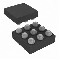
Manufacturer Part Number
DS2482X-101+T
Description
IC MASTER I2C-1WIRE 1CH 9-WLP
Manufacturer
Maxim Integrated Products
Datasheet
1.DS2482X-101T.pdf
(24 pages)
Specifications of DS2482X-101+T
Controller Type
I²C Bus Controller
Interface
I²C
Voltage - Supply
2.9 V ~ 5.5 V
Current - Supply
750µA
Operating Temperature
-40°C ~ 85°C
Mounting Type
Surface Mount
Package / Case
9-WLP
Lead Free Status / RoHS Status
Lead free / RoHS Compliant


Single-Channel 1-Wire Master with Sleep Mode
Figure 9. I
The following terminology is commonly used to
describe I
defined in Figure 9.
16
SDA
SCL
NOTE: TIMING IS REFERENCED TO V
Bus Idle or Not Busy: Both SDA and SCL are inac-
tive and in their logic-high states.
START Condition: To initiate communication with a
slave, the master must generate a START condition.
A START condition is defined as a change in state of
SDA from high to low while SCL remains high.
STOP Condition: To end communication with a
slave, the master must generate a STOP condition. A
STOP condition is defined as a change in state of
SDA from low to high while SCL remains high.
Repeated START Condition: Repeated STARTs are
commonly used for read accesses to select a spe-
cific data source or address to read from. The mas-
ter can use a repeated START condition at the end
of a data transfer to immediately initiate a new data
transfer following the current one. A repeated START
condition is generated the same way as a normal
START condition, but without leaving the bus idle
after a STOP condition.
Data Valid: With the exception of the START and
STOP condition, transitions of SDA can occur only
during the low state of SCL. The data on SDA must
remain valid and unchanged during the entire high
pulse of SCL plus the required setup and hold time
(t
HD:DAT
______________________________________________________________________________________
STOP
2
C Timing Diagram
2
t
BUF
C data transfers. The timing references are
after the falling edge of SCL and t
START
t
HD:STA
IL(MAX)
t
LOW
AND V
IH(MIN)
t
R
.
I
t
HD:DAT
2
C Definitions
t
HIGH
SU:DAT
t
F
t
SU:DAT
REPEATED
START
before the rising edge of SCL; see Figure 9). There
is one clock pulse per bit of data. Data is shifted into
the receiving device during the rising edge of SCL.
When finished with writing, the master must release
the SDA line for a sufficient amount of setup time
(minimum t
rising edge of SCL to start reading. The slave shifts
out each data bit on SDA at the falling edge of the
previous SCL pulse and the data bit is valid at the
rising edge of the current SCL pulse. The master
generates all SCL clock pulses, including those
needed to read from a slave.
Acknowledge: Typically a receiving device, when
addressed, is obliged to generate an acknowledge
after the receipt of each byte. The master must gen-
erate a clock pulse that is associated with this
acknowledge bit. A device that acknowledges must
pull SDA low during the acknowledge clock pulse in
such a way that SDA is stable low during the high
period of the acknowledge-related clock pulse plus
the required setup and hold time (t
falling edge of SCL and t
edge of SCL).
Not Acknowledged by Slave: A slave device may
be unable to receive or transmit data, for example,
because it is busy performing some real-time func-
tion or is in sleep mode. In this case, the slave
device does not acknowledge its slave address and
leaves the SDA line high. A slave device that is
ready to communicate acknowledges at least its
t
SU:STA
t
HD:STA
SU:DAT
+ t
SUPPRESSION
R
SPIKE
in Figure 9) before the next
SU:DAT
t
SP
before the rising
HD:DAT
t
SU:STO
after the
Related parts for DS2482X-101+T
Image
Part Number
Description
Manufacturer
Datasheet
Request
R

Part Number:
Description:
WLP/I°/SINGLE-CH 1-W LN DR LF UCSP PARTIAL
Manufacturer:
Maxim Integrated Products
Part Number:
Description:
WLP 8/I°/Single-Channel 1-Wire® Master with Sleep Mode
Manufacturer:
Maxim Integrated Products

Part Number:
Description:
IC MASTER I2C-1WIRE 1CH 9-WLP
Manufacturer:
Maxim Integrated Products
Datasheet:
Part Number:
Description:
MAX7528KCWPMaxim Integrated Products [CMOS Dual 8-Bit Buffered Multiplying DACs]
Manufacturer:
Maxim Integrated Products
Datasheet:
Part Number:
Description:
Single +5V, fully integrated, 1.25Gbps laser diode driver.
Manufacturer:
Maxim Integrated Products
Datasheet:
Part Number:
Description:
Single +5V, fully integrated, 155Mbps laser diode driver.
Manufacturer:
Maxim Integrated Products
Datasheet:
Part Number:
Description:
VRD11/VRD10, K8 Rev F 2/3/4-Phase PWM Controllers with Integrated Dual MOSFET Drivers
Manufacturer:
Maxim Integrated Products
Datasheet:
Part Number:
Description:
Highly Integrated Level 2 SMBus Battery Chargers
Manufacturer:
Maxim Integrated Products
Datasheet:
Part Number:
Description:
Current Monitor and Accumulator with Integrated Sense Resistor; ; Temperature Range: -40°C to +85°C
Manufacturer:
Maxim Integrated Products
Part Number:
Description:
TSSOP 14/A°/RS-485 Transceivers with Integrated 100O/120O Termination Resis
Manufacturer:
Maxim Integrated Products
Part Number:
Description:
TSSOP 14/A°/RS-485 Transceivers with Integrated 100O/120O Termination Resis
Manufacturer:
Maxim Integrated Products
Part Number:
Description:
QFN 16/A°/AC-DC and DC-DC Peak-Current-Mode Converters with Integrated Step
Manufacturer:
Maxim Integrated Products
Part Number:
Description:
TDFN/A/65V, 1A, 600KHZ, SYNCHRONOUS STEP-DOWN REGULATOR WITH INTEGRATED SWI
Manufacturer:
Maxim Integrated Products
Part Number:
Description:
Integrated Temperature Controller f
Manufacturer:
Maxim Integrated Products
Part Number:
Description:
SOT23-6/I°/45MHz to 650MHz, Integrated IF VCOs with Differential Output
Manufacturer:
Maxim Integrated Products