DS21FF44 Maxim Integrated Products, DS21FF44 Datasheet
DS21FF44
Specifications of DS21FF44
Available stocks


Related parts for DS21FF44

DS21FF44 Summary of contents
Page 1
... DESCRIPTION The and MCMs offer a high-density packaging arrangement for the DS21Q44 E1 enhanced quad framer. Either three (DS21FT44) or four (DS21FF44) silicon die of these devices is packaged in a multichip module (MCM) with the electrical connections as shown in Figure 1-1. All of the functions available on the DS21Q44 are also available in the MCM packaged version. ...
Page 2
... Changes from Normal DS21Q44 Configuration 1) TSYSCLK and RSYSCLK are connected together. 2) These signals are not available: RFSYNC/RLCLK/RLINK/RCHCLK/RMSYNC/RLOS/LOTC/TCHBLK/TLCLK/TLINK/TCHCLK Figure 1-1. DS21FT44/DS21FF44 SCHEMATIC See Connecting Page DS21Q44 # 1 DVSS DVSS Signals Not Connected & FMS Left Open Circuited Include: TLINK0/1/2/3 RLOS/LOTC RLINK RCLK1/2/3/4 TEST ...
Page 3
... Figure 1-1. DS21FF44/DS21FT44 SCHEMATIC (continued) See Connecting Page jtdot jtdof DS21Q44 # 3 DVSS DVSS CLKSI Signals Not Connected & FMS Left Open Circuited Include: RLOS/LOTC TLINK0/1/2/3 RLINK RCLK9/10/11/12 TEST RLCLK MUX RPOS9/10/11/12 RCHCLK RNEG9/10/11/12 BTS RMSYNC RFSYNC RSER9/10/11/12 FS0/FS1 TLCLK RSIG9/10/11/12 WR* ...
Page 4
... DESCRIPTION....................................................................................................................................1 2. MCM PIN DESCRIPTION ................................................................................................................7 3. DS21FF44 ( PCB LAND PATTERNS ....................................................................................15 4. DS21FT44 ( PCB Land Pattern ..............................................................................................16 5. DS21Q42 DIE DESCRIPTION ........................................................................................................17 6. DS21Q44 INTRODUCTION ............................................................................................................18 7. DS21Q44 PIN FUNCTION DESCRIPTION ..................................................................................20 8. DS21Q44 REGISTER MAP .............................................................................................................27 9. PARALLEL PORT ...........................................................................................................................32 10. CONTROL, ID, AND TEST REGISTERS.....................................................................................32 11. STATUS AND INFORMATION REGISTERS .............................................................................42 12 ...
Page 5
ADDITIONAL (Sa) AND INTERNATIONAL (Si) BIT OPERATION ......................................65 18.1 HARDWARE SCHEME ...............................................................................................................65 18.2 INTERNAL REGISTER SCHEME BASED ON DOUBLE–FRAME ........................................66 18.3 INTERNAL REGISTER SCHEME BASED ON CRC4 MULTIFRAME...................................68 19. HDLC CONTROLLER FOR THE SA BITS OR DS0 ..................................................................70 19.1 ...
Page 6
... Initial Release 122998 TEST and MUX pins were added at previous No Connect (NC) pins. 101899 DS21Q42 die specifications appended to data sheet. 020300 Conversion from Interleaf to Microsoft Word 120601 Updated DC Characteristics to show supply currents for DS21FT44/DS21FF44 062602 Updated device characterization data NOTES 6 of 117 ...
Page 7
MCM PIN DESCRIPTION Table 2-1. PIN DESCRIPTION SORTED BY SYMBOL PIN SYMBOL B7 8MCLK G20 A0 H20 A1 G19 A2 H19 A3 G18 A4 H18 A5 G17 A6 H17 A7 W15 BTS B6 CLKSI T8 CS1* Y4 CS2* Y15 ...
Page 8
PIN SYMBOL U8 DVSS2 U4 DVSS3 R16 DVSS3 Y20 DVSS3 J20 DVSS4/NC A11 DVSS4/NC D19 DVSS4/NC Y14 FS0 W14 FS1 G16 INT* V14 JTCLK E10 JTDI A19 JTDOF/NC T17 JTDOT H16 JTMS K17 JTRST* A13 TEST P17 MUX C2 RCHBLK1 ...
Page 9
PIN SYMBOL W10 RCLK10 Y18 RCLK11 N17 RCLK12 D14 RCLK13/NC P20 RCLK14/NC C18 RCLK15/NC C12 RCLK16/NC E18 RD* B2 RNEG1 H2 RNEG2 D9 RNEG3 A9 RNEG4 M2 RNEG5 V3 RNEG6 V7 RNEG7 P3 RNEG8 U9 RNEG9 W11 RNEG10 W17 RNEG11 ...
Page 10
PIN SYMBOL A14 RPOS16/NC C1 RSER1 H3 RSER2 C6 RSER3 C8 RSER4 P1 RSER5 W4 RSER6 T7 RSER7 N4 RSER8 U11 RSER9 Y12 RSER10 V16 RSER11 T16 RSER12 E16 RSER13/NC F20 RSER14/NC C16 RSER15/NC A12 RSER16/NC D3 RSIG1 G2 RSIG2 ...
Page 11
PIN SYMBOL U5 RSYNC7 J4 RSYNC8 T11 RSYNC9 V13 RSYNC10 V15 RSYNC11 P18 RSYNC12 J17 RSYNC13/NC J19 RSYNC14/NC B17 RSYNC15/NC B12 RSYNC16/NC B5 SYSCLK1 E2 SYSCLK2 E5 SYSCLK3 B8 SYSCLK4 M4 SYSCLK5 T2 SYSCLK6 Y5 SYSCLK7 W3 SYSCLK8 T4 SYSCLK9 ...
Page 12
PIN SYMBOL C3 TNEG1 J1 TNEG2 F5 TNEG3 A10 TNEG4 L1 TNEG5 V2 TNEG6 V8 TNEG7 P5 TNEG8 U14 TNEG9 V12 TNEG10 W18 TNEG11 T19 TNEG12 D11 TNEG13/NC K18 TNEG14/NC C19 TNEG15/NC B15 TNEG16/NC B3 TPOS1 J2 TPOS2 J5 TPOS3 ...
Page 13
PIN SYMBOL T3 TSER8 M16 TSER9 W9 TSER10 W16 TSER11 W20 TSER12 D13 TSER13/NC F17 TSER14/NC D18 TSER15/NC A18 TSER16/NC C4 TSIG1 F1 TSIG2 G4 TSIG3 C10 TSIG4 L3 TSIG5 U2 TSIG6 V9 TSIG7 R5 TSIG8 U15 TSIG9 V10 TSIG10 ...
Page 14
PIN SYMBOL A17 TSSYNC16/NC E3 TSYNC1 F4 TSYNC2 E7 TSYNC3 A4 TSYNC4 R2 TSYNC5 W5 TSYNC6 T5 TSYNC7 M5 TSYNC8 T13 TSYNC9 W13 TSYNC10 U16 TSYNC11 N16 TSYNC12 J16 TSYNC13/NC F18 TSYNC14/NC C15 TSYNC15/NC D12 TSYNC16/NC Y16 WR* I/O I ...
Page 15
... DS21FF44 ( PCB LAND PATTERNS The diagram shown below is the pin pattern that is placed on the target PCB. This is the same pattern that would be seen as viewed through the MCM from the top. Figure 3-1. PIN PATTERN FOR TARGET PCB ( rpos rclk ts tsync tclk ...
Page 16
DS21FT44 (Four x Three) PCB Land Pattern The diagram shown below is the pin pattern that is placed on the target PCB. This is the same pattern that would be seen as viewed through the MCM from the top. ...
Page 17
DS21Q44 DIE DESCRIPTION FEATURES § Four E1 (CEPT or PCM-30)/ISDN-PRI framing transceivers § All four framers are fully independent; transmit and receive sections of each framer are fully independent § Frames to FAS, CAS, CCS, and CRC4 formats § ...
Page 18
DS21Q44 INTRODUCTION The DS21Q44 is a superset version of the popular DS21Q43 quad E1 framer offering the new features listed below. All of the original features of the DS21Q43 have been retained and software created for the original device ...
Page 19
Figure 6-1. DS21Q44 ENHANCED QUAD E1 FRAMER Receive Side Framer RPOS RCLK RNEG Transmit Side Formatter TPOS TNEG FRAMER #0 FRAMER #1 FRAMER #2 FRAMER #3 CLKS I 3 VDD Power 3 VSS TEST CS* FS0 FS1 Note: 1. Alternate ...
Page 20
... Only used when the transmit side elastic store function is enabled. Should be connected low in applications that do not use the transmit side elastic store. Can be burst at rates up to 8.192MHz. This pin is connected to the RSYSCLK signal in the DS21FF44/DS21FT44. Signal Name: TLCLK ...
Page 21
... When enabled, this input will sample signaling bits for insertion into outgoing PCM E1 data stream. Sampled on the falling edge of TCLK when the transmit side elastic store is disabled. Sampled on the falling edge of TSYSCLK when the transmit side elastic store is enabled. This function is available when FMS = 0. FMS is connected to ground for the DS21FF44/DS21FT44. Signal Name: TPOS ...
Page 22
... A 256kHz clock that pulses high during the LSB of each channel. Synchronous with RCLK when the receive side elastic store is disabled. Synchronous with RSYSCLK when the receive side elastic store is enabled. Useful for parallel to serial conversion of channel data. This function is available when FMS = 1 (DS21Q43 emulation). This signal is not bonded out in the DS21FF44/DS21FT44. Signal Name: RCHBLK ...
Page 23
... Outputs signaling bits in a PCM format. Updated on rising edges of RCLK when the receive side elastic store is disabled. Updated on the rising edges of RSYSCLK when the receive side elastic store is enabled. This function is available when FMS = 0. FMS is connected to ground for the DS21FF44/DS21FT44. Signal Name: ...
Page 24
... Signal Name: FMS Signal Description: Framer Mode Select Signal Type: Input Set low to select DS21Q44 feature set. Set high to select DS21Q43 emulation. FMS is connected to ground for the DS21FF44/DS21FT44. Signal Name: MUX Signal Description: Bus Operation Signal Type: Input Set low to select nonmultiplexed bus operation. Set high to select multiplexed bus operation. ...
Page 25
... This action sets the device into the boundary scan bypass mode allowing normal device operation. If boundary scan is not used, this pin should be held low. This function is available when FMS = 0. FMS is connected to ground for the DS21FF44/DS21FT44. Signal Name: ...
Page 26
... Signal Type: Output Test instructions and data are clocked out of this pin on the falling edge of JTCLK. If not used, this pin should be left unconnected. This function is available when FMS = 0. FMS is connected to ground for the DS21FF44/DS21FT44. SUPPLY PINS Signal Name: VDD Signal Description: ...
Page 27
... Transmit Channel Blocking 4 26 R/W Transmit Idle 1 27 R/W Transmit Idle 2 28 R/W Transmit Idle 3 29 R/W Transmit Idle 4 REGISTER NAME 27 of 117 DS21FT44/DS21FF44 SYMBOL VCR1 VCR2 CRCCR1 CRCCR2 EBCR1 EBCR2 SR1 SR2 RIR TEST2 (set to 00h) (set to 00H) (set to 00H) (set to 00H) ...
Page 28
... R/W Transmit Sa4 Bits 54 R/W Transmit Sa5 Bits 55 R/W Transmit Sa6 Bits 56 R/W Transmit Sa7 Bits 57 R/W Transmit Sa8 Bits REGISTER NAME 28 of 117 DS21FT44/DS21FF44 SYMBOL TIDR RCBR1 RCBR2 RCBR3 RCBR4 RAF RS1 RS2 RS3 RS4 RS5 RS6 RS7 RS8 RS9 ...
Page 29
... R/W Receive Channel 2 82 R/W Receive Channel 3 83 R/W Receive Channel 4 84 R/W Receive Channel 5 85 R/W Receive Channel 6 REGISTER NAME 29 of 117 DS21FT44/DS21FF44 SYMBOL RSiAF RSiNAF RRA RSa4 RSa5 RSa6 RSa7 RSa8 TC1 TC2 TC3 TC4 TC5 TC6 TC7 TC8 ...
Page 30
... Not Used B0 R/W HDLC Control Register B1 R/W HDLC Status Register B2 R/W HDLC Interrupt Mask Register B3 R/W Receive HDLC Information Register REGISTER NAME 30 of 117 DS21FT44/DS21FF44 SYMBOL RC7 RC8 RC9 RC10 RC11 RC12 RC13 RC14 RC15 RC16 RC17 RC18 RC19 RC20 ...
Page 31
... Test Registers 1, 2, and 3 are used only by the factory; these registers must be cleared (set to all 0’s) on power-up initialization to ensure proper operation. 2) Register banks CxH, DxH, ExH, and FxH are not accessible. REGISTER NAME 31 of 117 DS21FT44/DS21FF44 SYMBOL RHFR IBO THIR THFR ...
Page 32
... When emulating the DS21Q43 feature set (FMS = 1), the full address space (00H through 0BFH) must be initialized. DS21Q43 emulation require address pin used. FMS is connected to ground for the DS21FF44/DS21FT44. Finally, after the TSYSCLK and RSYSCLK inputs are stable, the ESR bit should be toggled from a zero to a one (this step can be skipped if the elastic stores are disabled) ...
Page 33
IDR: DEVICE IDENTIFICATION REGISTER (Address = 0F Hex) (MSB) T1E1 0 SYMBOL POSITION T1E1 IDR.7 ID3 IDR.3 ID2 IDR.1 ID1 IDR.2 ID0 IDR.0 RCR1: RECEIVE CONTROL REGISTER 1 (Address = 10 Hex) (MSB) RSMF RSM SYMBOL POSITION RSMF RCR1.7 RSM ...
Page 34
Table 10–1. SYNC/RESYNC CRITERIA FRAME OR MULTIFRAME SYNC CRITERIA LEVEL FAS present in frame N FAS and and FAS not present in frame Two valid MF alignment CRC4 words found within 8 ms Valid ...
Page 35
TCR1: TRANSMIT CONTROL REGISTER 1 (Address = 12 Hex) (MSB) ODF TFPT SYMBOL POSITION ODF TCR1.7 TFPT TCR1.6 T16S TCR1.5 TUA1 TCR1.4 TSiS TCR1.3 TSA1 TCR1.2 TSM CR1.1 TSIO TCR1.0 Note: See Figure 22–15 for more details about how the ...
Page 36
TCR2: TRANSMIT CONTROL REGISTER 2 (Address = 13 Hex) (MSB) Sa8S Sa7S SYMBOL POSITION Sa8S TCR2.7 Sa7S TCR2.6 Sa6S TCR2.5 Sa5S TCR2.4 Sa4S TCR2.3 ODM TCR2.2 AEBE TCR2.1 PF TCR2.0 Sa6S Sa5S Sa4S NAME AND DESCRIPTION Sa8 Bit Select. Set ...
Page 37
CCR1: COMMON CONTROL REGISTER 1 (Address = 14 Hex) (MSB) FLB THDB3 TG802 SYMBOL POSITION FLB CCR1.7 THDB3 CCR1.6 TG802 CCR1.5 TCRC4 CCR1.4 RSM CCR1.3 RHDB3 CCR1.2 RG802 CCR1.1 RCRC4 CCR1.0 FRAMER LOOPBACK When CCR1.7 is set to a one, ...
Page 38
CCR2: COMMON CONTROL REGISTER 2 (Address = 1A Hex) (MSB) ECUS VCRFS AAIS SYMBOL POSITION ECUS CCR2.7 VCRFS CCR2.6 AAIS CCR2.5 ARA CCR2.4 RSERC CCR2.3 LOTCMC CCR2.2 RFF CCR2.1 RFE CCR2.0 AUTOMATIC ALARM GENERATION The DS21Q44 can be programmed to ...
Page 39
Remote Alarm will be transmitted if the framer cannot find CRC4 multiframe synchronization within 400ms as per G.706 illegal state to have both CCR2.4 and CCR2.5 set to one at the same time. CCR3: COMMON CONTROL ...
Page 40
CCR4: COMMON CONTROL REGISTER 4 (Address = A8 Hex) (MSB) RLB — SYMBOL POSITION RLB CCR4.7 — CCR4.6 — CCR4.5 TCM4 CCR4.4 TCM3 CCR4.3 TCM2 CCR4.2 TCM1 CCR4.1 TCM0 CCR4.0 — TCM4 TCM3 NAME AND DESCRIPTION Remote Loopback 0 = ...
Page 41
CCR5: COMMON CONTROL REGISTER 5 (Address = AA Hex) (MSB) — RESALGN TESALGN SYMBOL POSITION — CCR5.7 RESALGN CCR5.6 TESALGN CCR5.5 RCM4 CCR5.4 RCM3 CCR5.3 RCM2 CCR5.2 RCM1 CCR5.1 RCM0 CCR5.0 RCM4 RCM3 RCM2 NAME AND DESCRIPTION Not Assigned. Should ...
Page 42
CCR6: COMMON CONTROL REGISTER 6 (Address = 1D Hex) (MSB) — — SYMBOL POSITION — CCR6.7 — CCR6.6 — CCR6.5 — CCR6.4 — CCR6.3 TCLKSRC CCR6.2 RESR CCR6.1 TESR CCR6.0 11. STATUS AND INFORMATION REGISTERS There is a set of ...
Page 43
The read result should be logically AND’ed with the mask byte that was just written and this value should be written back into ...
Page 44
ISR: INTERRUPT STATUS REGISTER (Any address from 0C0 Hex to 0FF Hex) (MSB) F3HDLC F3SR F2HDLC SYMBOL POSITION F3HDLC ISR.7 F3SR ISR.6 F2HDLC ISR.5 F2SR ISR.4 F1HDLC ISR.3 F1SR ISR.2 F0HDLC ISR.1 F0SR ISR.0 F2SR F1HDLC F1SR NAME AND DESCRIPTION ...
Page 45
RIR: RECEIVE INFORMATION REGISTER (Address = 08 Hex) (MSB) TESF TESE LORC SYMBOL POSITION TESF RIR.7 TESE RIR.6 LORC RIR.5 RESF RIR.4 RESE RIR.3 CRCRC RIR.2 FASRC RIR.1 CASRC RIR.0 SSR: SYNCHRONIZER STATUS REGISTER (Address = 1E Hex) (MSB) CSC5 ...
Page 46
CRC4 level cannot be obtained within 400ms, then the search should be abandoned and proper action taken. The CRC4 Sync Counter rolls over. SR1: STATUS REGISTER 1 (Address = 06 Hex) (MSB) RSA1 RDMA RSA0 ...
Page 47
... MF More than two 0’s in two frames (512 bits) Bit 3 of nonalign frame set to 0 for three consecutive occasions In 255 bit times, at least 32 1’s are received 47 of 117 DS21FT44/DS21FF44 ITU SPEC. G.732 4.2 G.732 5.2 O.162 2.1.5 O.162 1 ...
Page 48
SR2: STATUS REGISTER 2 (Address = 07 Hex) (MSB) RMF RAF SYMBOL POSITION RMF SR2.7 RAF SR2.6 TMF SR2.5 SEC SR2.4 TAF SR2.3 LOTC SR2.2 RCMF SR2.1 TSLIP SR2.0 TMF SEC TAF NAME AND DESCRIPTION Receive CAS Multiframe. Set every ...
Page 49
IMR1: INTERRUPT MASK REGISTER 1 (Address = 16 Hex) (MSB) RSA1 RDMA RSA0 SYMBOL POSITION RSA1 IMR1.7 RDMA IMR1.6 RSA0 IMR1.5 RSLIP IMR1.4 RUA1 IMR1.3 RRA IMR1.2 RCL IMR1.1 RLOS IMR1.0 RSLIP RUA1 RRA NAME AND DESCRIPTION Receive Signaling All ...
Page 50
IMR2: INTERRUPT MASK REGISTER 2 (Address = 17 Hex) (MSB) RMF RAF SYMBOL POSITION RMF IMR2.7 RAF IMR2.6 TMF IMR2.5 SEC IMR2.4 TAF IMR2.3 LOTC IMR2.2 RCMF IMR2.1 TSLIP IMR2.0 12. ERROR COUNT REGISTERS There are a set of four ...
Page 51
HDB3 code. This counter increments at all times and is not disabled by loss of sync conditions. The counter saturates at 65,535 and will not rollover. The bit error rate line would have to be greater ...
Page 52
E-Bit Counter E-bit Count Register 1 (EBCR1) is the most significant word and EBCR2 is the least significant word of a 10-bit counter that records Far End Block Errors (FEBE) as reported in the first bit of frames 13 and ...
Page 53
DS0 MONITORING FUNCTION Each framer in the DS21Q44 has the ability to monitor one DS0 64kbps channel in the transmit direction and one DS0 channel in the receive direction at the same time. In the transmit direction, the user ...
Page 54
CCR4: COMMON CONTROL REGISTER 4 (Address=A8 Hex) [Repeated here from section 10 for convenience] (MSB) RLB – SYMBOL POSITION RLB CCR4.7 — CCR4.6 — CCR4.5 TCM4 CCR4.4 TCM3 CCR4.3 TCM2 CCR4.2 TCM1 CCR4.1 TCM0 CCR4.0 TDS0M: TRANSMIT DS0 MONITOR REGISTER ...
Page 55
CCR5: COMMON CONTROL REGISTER 5 (Address = AA Hex) (Repeated here from Section 10.) (MSB) — RESALGN TESALGN SYMBOL POSITION – CCR5.7 RESALGN CCR5.6 TESALGN CCR5.5 RCM4 CCR5.4 RCM3 CCR5.3 RCM2 CCR5.2 RCM1 CCR5.1 RCM0 CCR5.0 RCM4 RCM3 RCM2 NAME ...
Page 56
RDS0M: RECEIVE DS0 MONITOR REGISTER (Address = AB Hex) (MSB SYMBOL POSITION B1 RDS0M.7 B2 RDS0M.6 B3 RDS0M.5 B4 RDS0M.4 B5 RDS0M.3 B6 RDS0M.2 B7 RDS0M.1 B8 RDS0M.0 14. SIGNALING OPERATION Each framer in the DS21Q44 contains provisions ...
Page 57
RS1 TO RS16: RECEIVE SIGNALING REGISTERS (Address = Hex) (MSB A(1) B(1) C(1) A(2) B(2) C(2) A(3) B(3) C(3) A(4) B(4) C(4) A(5) B(5) C(5) A(6) B(6) C(6) A(7) B(7) C(7) A(8) B(8) C(8) ...
Page 58
TS1 TO TS16: TRANSMIT SIGNALING REGISTERS (Address = Hex) (MSB A(1) B(1) C(1) A(2) B(2) C(2) A(3) B(3) C(3) A(4) B(4) C(4) A(5) B(5) C(5) A(6) B(6) C(6) A(7) B(7) C(7) A(8) B(8) C(8) ...
Page 59
Hardware-Based Signaling Receive Side In the receive side of the hardware based signaling, there are two operating modes for the signaling buffer; signaling extraction and signaling re–insertion. Signaling extraction involves pulling the signaling bits from the receive data stream ...
Page 60
TCBR1/TCBR2/TCBR3/TCBR4: DEFINITION WHEN CCR3 (MSB) CH20 CH4 CH19 CH24 CH8 CH23 CH28 CH12 CH27 CH32 CH16 CH31 *CH1 and CH17 should be set to one to allow the internal TS1 register to create the CAS Multiframe Alignment Word ...
Page 61
The Transmit Idle Registers (TIRs) have an alternate function that allow them to define a Per–Channel LoopBack (PCLB). If the TIRFS control bit (CCR3.5) is set to one, then the TIRs will determine which channels (if any) from the backplane ...
Page 62
TC1 TO TC32: TRANSMIT CHANNEL REGISTERS (Address = Hex) (for brevity, only channel one is shown; see Table 8-1 for other register address) (MSB SYMBOL POSITION C7 TC1.7 C0 TC1.0 TCC1/TCC2/TCC3/TCC4: TRANSMIT CHANNEL CONTROL ...
Page 63
RCC1/RCC2/RCC3/RCC4: RECEIVE CHANNEL CONTROL REGISTER (Address = Hex) (MSB) CH8 CH7 CH6 CH16 CH15 CH14 CH24 CH23 CH22 CH32 CH31 CH30 SYMBOL POSITION CH1–32 RCC1.0–4.7 16. CLOCK BLOCKING REGISTERS The Receive Channel blocking Registers (RCBR1/RCBR2/RCBR3/RCBR4) and the ...
Page 64
TCBR1/TCBR2/TCBR3/TCBR4: TRANSMIT CHANNEL BLOCKING REGISTERS (Address = Hex) (MSB) CH8 CH7 CH6 CH16 CH15 CH14 CH24 CH23 CH22 CH32 CH31 CH30 SYMBOL POSITION CH1–32 TCBR1.0–4.7 Note: If CCR3 then a zero in the TCBRs implies ...
Page 65
Receive Side If the receive side elastic store is enabled (RCR2.1=1), then the user must provide either a 1.544MHz (RCR2.2 =0) or 2.048MHz (RCR2.2=1) clock at the RSYSCLK pin. The user has the option of either providing a frame/multiframe ...
Page 66
Internal Register Scheme Based On Double-Frame On the receive side, the RAF and RNAF registers will always report the data as it received in the Additional and International bit locations. The RAF and RNAF registers are updated with the ...
Page 67
TAF: TRANSMIT ALIGN FRAME REGISTER (Address = 20 Hex) (MSB (Must be programmed with the 7-bit FAS word; the DS21Q44 does not automatically set these bits.) SYMBOL POSITION Si TAF.7 0 TAF.6 0 TAF.5 1 TAF.4 1 TAF.3 ...
Page 68
... The eight settings of remote alarm (RA). 53 The eight Sa4 settings in each CRC4 multiframe. 54 The eight Sa5 settings in each CRC4 multiframe. 55 The eight Sa6 settings in each CRC4 multiframe. 56 The eight Sa7 settings in each CRC4 multiframe. 57 The eight Sa8 settings in each CRC4 multiframe 117 DS21FT44/DS21FF44 FUNCTION ...
Page 69
TSaCR: TRANSMIT Sa BIT CONTROL REGISTER (Address = 1C Hex) (MSB) SiAF SiNAF SYMBOL POSITION SiAF TSaCR.7 SiNAF TSaCR.6 RA TSaCR.5 Sa4 TSaCR.4 Sa5 TSaCR.3 Sa6 TSaCR.2 Sa7 TSaCR.1 Sa8 TSaCR.0 RA Sa4 Sa5 NAME AND DESCRIPTION International Bit in ...
Page 70
HDLC Controller for the Sa Bits or DS0 Each framer in the DS21Q44 has the ability to extract/insert data from/ into the Sa bit positions (Sa4 to Sa8) or from/to any multiple of DS0 channels Each framer contains a ...
Page 71
... Status information on receive HDLC controller Access to 64-byte HDLC FIFO in receive direction Controls the HDLC function when used on DS0 channels Status information on transmit HDLC controller Access to 64–byte HDLC FIFO in transmit direction Controls the HDLC function when used on DS0 channels 71 of 117 DS21FT44/DS21FF44 ...
Page 72
The read result should be logically AND’ed with the mask byte that was just written and this value should be written back into the same register to insure that bit does indeed clear. This second write step is necessary ...
Page 73
HDLC REGISTER DESCRIPTION HCR: HDLC CONTROL REGISTER (Address=B0 Hex) (MSB) — RHR SYMBOL POSITION — HCR.7 RHR HCR.6 TFS HCR.5 THR HCR.4 TABT HCR.3 TEOM HCR.2 TZSD HCR.1 TCRCD HCR.0 TFS THR TABT NAME AND DESCRIPTION Not Assigned. Should ...
Page 74
HSR: HDLC STATUS REGISTER (Address = B1 Hex) (MSB) — RPE SYMBOL POSITION — HSR.7 RPE HSR.6 RPS HSR.5 RHALF HSR.4 RNE HSR.3 THALF HSR.2 TNF HSR.1 TMEND HSR.0 Note: The RPE, RPS, and TMEND bits are latched and are ...
Page 75
HIMR: HDLC INTERRUPT MASK REGISTER (Address = B2 Hex) (MSB) — RPE SYMBOL POSITION — HIMR.7 RPE HIMR.6 RPS HIMR.5 RHALF HIMR.4 RNE HIMR.3 THALF HIMR.2 TNF HIMR.1 TMEND HIMR.0 RPS RHALF RNE NAME AND DESCRIPTION Not Assigned. Should be ...
Page 76
RHIR: RECEIVE HDLC INFORMATION REGISTER (Address = B3 Hex) (MSB) RABT RCRCE ROVR SYMBOL POSITION RABT RHIR.7 RCRCE RHIR.6 ROVR RHIR.5 RVM RHIR.4 REMPTY RHIR.3 POK RHIR.2 CBYTE RHIR.1 OBYTE RHIR.0 Note: The RABT, RCRCE, ROVR, and RVM bits are ...
Page 77
THIR: TRANSMIT HDLC INFORMATION REGISTER (Address = B6 Hex) (MSB) — — SYMBOL POSITION — THIR.7 — THIR.6 — THIR.5 — THIR.4 — THIR.3 TEMPTY THIR.2 TFULL THIR.1 TUDR THIR.0 Note: The TUDR bit is latched and are cleared when ...
Page 78
RDC1: RECEIVE HDLC DS0 CONTROL REGISTER 1 (Address = B8 Hex) (MSB) RHS RSaDS RDS0M SYMBOL POSITION RHS RDC1.7 RSaDS RDC1.6 RDS0M RDC1.5 RD4 RDC1.4 RD3 RDC1.3 RD2 RDC1.2 RD1 RDC1.1 RD0 RDC1.0 RD4 RD3 RD2 NAME AND DESCRIPTION Receive ...
Page 79
RDC2: RECEIVE HDLC DS0 CONTROL REGISTER 2 (Address = B9 Hex) (MSB) RDB8 RDB7 RDB6 SYMBOL POSITION RDB8 RDC2.7 RDB7 RDC2.6 RDB6 RDC2.5 RDB5 RDC2.4 RDB4 RDC2.3 RDB3 RDC2.2 RDB2 RDC2.1 RDB1 RDC2.0 RDB5 RDB4 RDB3 NAME AND DESCRIPTION DS0 ...
Page 80
TDC1: TRANSMIT HDLC DS0 CONTROL REGISTER 1 (Address = BA Hex) (MSB) THE TSaDS TDS0M SYMBOL POSITION THE TDC1.7 TSaDS TDC1.6 TDS0M TDC1.5 TD4 TDC1.4 TD3 TDC1.3 TD2 TDC1.2 TD1 TDC1.1 TD0 TDC1.0 TD4 TD3 TD2 NAME AND DESCRIPTION Transmit ...
Page 81
TDC2: TRANSMIT HDLC DS0 CONTROL REGISTER 2 (Address = BB Hex) (MSB) TDB8 TDB7 TDB6 SYMBOL POSITION TDB8 TDC2.7 TDB7 TDC2.6 TDB6 TDC2.5 TDB5 TDC2.4 TDB4 TDC2.3 TDB3 TDC2.2 TDB2 TDC2.1 TDB1 TDC2.0 20. INTERLEAVED PCM BUS OPERATION In many ...
Page 82
IBO: INTERLEAVE BUS OPERATION REGISTER (Address = B5 Hex) (MSB) — —– SYMBOL POSITION — IBO.7 — IBO.6 — IBO.5 — IBO.4 IBOEN IBO.3 INTSEL IBO.2 MSEL0 IBO.1 MSEL1 IBO.0 Table 20-1. MASTER DEVICE BUS SELECT MSEL1 MSEL0 0 0 ...
Page 83
Figure 20-1. 4.096MHz INTERLEAVED BUS EXTERNAL PIN CONNECTION EXAMPLE FRAMER 0 FRAMER 1 RSYSCLK0 RSYSCLK1 TSYSCLK0 TSYSCLK1 RSYNC0 RSYNC1 TSSYNC0 TSSYNC1 RSER0 RSER1 TSER0 TSER1 RSIG0 RSIG1 TSIG0 TSIG1 Bus 1 Figure 20-2. 8.192MHz INTERLEAVED BUS EXTERNAL PIN CONNECTION EXAMPLE ...
Page 84
... IDCODE. See Figure 21-1 for a block diagram. The DS21Q44 contains the following items which meet the requirements set by the IEEE 1149.1 Standard Test Access Port and Boundary Scan Architecture. The DS21FT42 should be considered as 3 individual DS21Q42 devices. The DS21FF44 should be considered as 4 individual DS21Q44 devices. ...
Page 85
TAP CONTROLLER STATE MACHINE This section covers the details on the operation of the Test Access Port (TAP) Controller State Machine. Please see Figure 21.2 for details on each of the states described below. TAP Controller The TAP controller ...
Page 86
Update-DR A falling edge on JTCLK while in the Update-DR state will latch the data from the shift register path of the Test registers into the data output latches. This prevents changes at the parallel output due to changes in ...
Page 87
... DR-Scan IR-Scan Capture DR Capture IR 0 Shift DR Shift Exit DR Exit IR 0 Pause DR Pause Exit2 DR Exit2 IR 1 Update DR Update SELECTED REGISTER Boundary Scan Bypass Boundary Scan Boundary Scan Boundary Scan Device Identification 87 of 117 DS21FT44/DS21FF44 INSTRUCTION CODE 010 111 000 011 100 001 ...
Page 88
SAMPLE/PRELOAD A mandatory instruction for the IEEE 1149.1 specification. This instruction supports two functions. The digital I/Os of the DS21Q44 can be sampled at the boundary scan register without interfering with the normal operation of the device by using the ...
Page 89
TEST REGISTERS IEEE 1149.1 requires a minimum of two test registers; the bypass register and the boundary scan register. An optional test register has been included with the DS21Q44 design. This test register is the identification register and is ...
Page 90
Table 21-4. BOUNDARY SCAN REGISTER DESCRIPTION MCM MCM MCM PIN PIN PIN (DIE1) (DIE2) (DIE3) B7 G20 G20 G20 H20 H20 H20 G19 G19 G19 H19 H19 H19 G18 G18 G18 H18 H18 H18 G17 G17 G17 H17 H17 H17 ...
Page 91
MCM MCM MCM PIN PIN PIN (DIE1) (DIE2) (DIE3 T10 H1 W2 V11 H4 V5 Y19 C9 P4 R19 C1 P1 U11 H3 W4 Y12 C6 T7 V16 C8 N4 T16 D3 N2 U10 G2 V4 Y11 D4 ...
Page 92
MCM MCM MCM PIN PIN PIN (DIE1) (DIE2) (DIE3 M16 W16 D7 T3 W20 C4 L3 U15 F1 U2 V10 G4 V9 U18 C10 R5 R18 A3 L4 T15 ...
Page 93
TIMING DIAGRAMS Figure 22-1. RECEIVE SIDE TIMING FRAME# 1 RSYNC / RFSYNC 2 RSYNC 3 RLCLK 4 RLINK Notes: 1. RSYNC in the frame mode (RCR1 RSYNC in the multiframe ...
Page 94
Figure 22-3. RECEIVE SIDE 1.544MHz BOUNDARY TIMING (With Elastic Store Enabled) RSYSCLK CHANNEL 23/31 1 RSER 2 RSYNC / RMSYNC 3 RSYNC RCHCLK 4 RCHBLK Notes: 1. Data from the E1 channels 13, 17, 21, 25, and ...
Page 95
Figure 22-5. RECEIVE SIDE, INTERLEAVED BUS OPERATION BYTE MODE TIMING RSYNC 1 RSER FR1 CH32 FR0 CH1 1 RSIG FR1 CH32 FR0 CH1 2 RSER FR2 CH32 FR3 CH32 FR0 CH1 2 RSIG FR2 CH32 FR3 CH32 FR0 CH1 SYSCLK ...
Page 96
Figure 22-6. RECEIVE SIDE, INTERLEAVED BUS OPERATION FRAME MODE TIMING RSYNC 1 FR1 CH1-32 FR0 CH1-32 RSER 1 FR1 CH1-32 FR0 CH1-32 RSIG 2 RSER FR2 CH1-32 FR3 CH1-32 FR0 CH1-32 2 RSIG FR2 CH1-32 FR3 CH1-32 FR0 CH1-32 SYSCLK ...
Page 97
Figure 22-8. TRANSMIT SIDE BOUNDARY TIMING (With Elastic Store Disabled) TCLK TSER LSB Si 1 CHANNEL 32 1 TPOS, TNEG MSB 2 TSYNC 3 TSYNC TSIG TCHCLK 4 TCHBLK 5 TLCLK Don't Care 5 TLINK Notes: 1. ...
Page 98
Figure 22-10. TRANSMIT SIDE 2.048MHz BOUNDARY TIMING (With Elastic Store Enabled) TSYSCLK CHANNEL 31 TSER TSSYNC CHANNEL 31 TSIG TCHCLK 1 TCHBLK Notes: 1. TCHBLK is programmed to block channel 31 Figure 22-11. G.802 TIMING TIMESLOT # ...
Page 99
Figure 22-12. TRANSMIT SIDE, INTERLEAVED BUS OPERATION BYTE MODE TIMING TSSYNC 1 TSER FR1 CH32 FR0 CH1 1 FR1 CH32 FR0 CH1 TSIG 2 FR2 CH32 FR3 CH32 FR0 CH1 TSER 2 TSIG FR2 CH32 FR3 CH32 FR0 CH1 SYSCLK ...
Page 100
Figure 22-13. TRANSMIT SIDE INTERLEAVED BUS OPERATION FRAME MODE TIMING TSSYNC 1 FR1 CH1-32 FR0 CH1-32 TSER 1 FR0 CH1-32 TSIG FR1 CH1-32 2 TSER FR2 CH1-32 FR3 CH1-32 FR0 CH1-32 2 TSIG FR2 CH1-32 FR3 CH1-32 FR0 CH1-32 SYSCLK ...
Page 101
Figure 22-14. DS21Q44 FRAMER SYNCHRONIZATION FLOWCHART RLOS = 1 Resync if RCR1 Increment CRC4 Sync Counter; CRC4SA = 0 Set FASRC (RIR.1) CRC4 Resync Criteria Met (RIR.2) CAS Resync Criteria Met; Set CASRC (RIR.0) 8ms CRC4 Multiframe Search ...
Page 102
Figure 22-15. DS21Q44 TRANSMIT DATA FLOW 1/2/3 3 3.2 TNAF.0 ata S ource ( TNAF.5 /TN A ...
Page 103
... DS21FF44N/DS21FT44N) A MIN TYP V 2 -0.3 IL 2.97 DD MIN TYP OUT (V = 2.97 to 3.63V 0°C to +70°C for DS21FF44/DS21FT44 2.97 to 3.63V -40ºC to +85ºC for DS21FF44N/DS21FT44N) A MIN TYP I 225 DD I 300 +4.0 OL 103 of 117 DS21FT44/DS21FF44 -1.0V to +5.5V -0.3V to +3.63V 0º ...
Page 104
... Pulse Width AS or ALE PW high Delay time ALE t to DS, WR* or RD* Output Data Delay time from DS or RD* Data Setup time See Figures 23-1 to 23-3 for details = 2.97 to 3.63V 0°C to +70°C for DS21FF44/DS21FT44 -40°C to +85°C for DS21FF44N/DS21FT44N) A MIN TYP t 200 CYC 100 ...
Page 105
... Data Setup Time to either WR* or DS* Inactive Data Hold Time from either WR* or DS* Inactive Address Hold from either WR* or DS* inactive See Figures 23–4 to 23–7 for details 2.97 to 3.63V 0°C to +70°C for DS21FF44/DS21FT44 2.97 to 3.63V -40°C to +85°C for DS21FF44N/DS21FTN44) A MIN TYP ...
Page 106
... RSYNC, RCHBLK, RFSYNC, RLCLK Delay RSYSCLK to RSER, RSIG Valid Delay RSYSCLK to RCHCLK, RCHBLK, RMSYNC, RSYNC See Figures 23-8 to 23-10 for details. NOTES: 1) RSYSCLK = 1.544MHz 2) RSYSCLK = 2.048MHz (V = 2.97 to 3.63V 0°C to +70°C for DS21FF44/DS21FT44 -40°C to +85°C for DS21FF44N/DS21FT44N) A SYMBOL MIN TYP t 488 ...
Page 107
... TNEG Valid Delay TCLK to TCHBLK, TCHCLK, TSYNC, TLCLK Delay TSYSCLK to TCHCLK, TCHBLK See Figures 23–11 to 23–13 for details. NOTES: 1) TSYSCLK = 1.544MHz 2) TSYSCLK = 2.048MHz (V = 2.97 to 3.63V 0°C to +70°C for DS21FF44/DS21FT44 2.97 to 3.63V -40°C to +85°C for DS21FF44N/DS21FT44N) A MIN TYP t 488 CP t ...
Page 108
Figure 23-1. INTEL BUS READ AC TIMING (BTS = 0 / MUX = 1) ALE PW t ASD WR* t ASD RD CS* t ASL AD0-AD7 Figure 23-2. INTEL BUS WRITE TIMING (BTS = 0 / MUX = ...
Page 109
Figure 23-3. MOTOROLA BUS AC TIMING (BTS = 1 / MUX = ASD R/W* t ASL AD0-AD7 (read) t CS* t ASL AD0-AD7 (write) t AHL Figure 23-4. INTEL BUS READ AC TIMING ...
Page 110
Figure 23-5. INTEL BUS WRITE AC TIMING (BTS = 0 / MUX = A7, Address Valid FS0, FS1 RD* t1 0ns min. CS* 0ns min. WR* Figure 23-6. MOTOROLA BUS READ AC TIMING (BTS ...
Page 111
Figure 23-7. MOTOROLA BUS WRITE AC TIMING (BTS = 1 / MUX = A7, Address Valid FS0, FS1 R/W* t1 CS* 0ns min. DS* 0ns min Notes: 1. The signal DS is ...
Page 112
Figure 23-8. RECEIVE SIDE AC TIMING RCLK t D1 RSER / RSIG t D2 RCHCLK RCHBLK RFSYNC / RMSYNC 1 RSYNC RLCLK t D1 Sa4 to Sa8 Bit Position RLINK Notes: 1. RSYNC is in the output ...
Page 113
Figure 23-9. RECEIVE SYSTEM SIDE AC TIMING RSYSCLK t D3 RSER / RSIG t D4 RCHCLK RCHBLK SYNC RSYNC RSYNC N otes ...
Page 114
Figure 23-10. RECEIVE LINE INTERFACE AC TIMING RCLK RPOS, RNEG Figure 23-11. TRANSMIT SIDE AC TIMING TCLK TSER / TSIG t D2 TCHCLK TCHBLK TSYNC TSYNC ...
Page 115
Figure 23-12. TRANSMIT SYSTEM SIDE AC TIMING TSYSCLK TSER t D3 TCHCLK TCHBLK t SU TSS YNC N otes only sam pled on the falling edge ...
Page 116
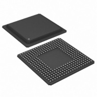
Figure 23-13. TRANSMIT LINE INTERFACE SIDE AC TIMING TCLK TPOS, TNEG t DD 24. MCM PACKAGE DIMENSIONS 116 of 117 ...
Page 117
POWER SUPPLY DECOUPLING In a typical PCB layout for the MCM, all of the VDD pins will connect to a common power plane and all the VSS lines will connect to a common ground plane. The recommended method for decoupling ...