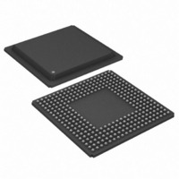
DS21FF44 Maxim Integrated Products, DS21FF44 Datasheet - Page 58

DS21FF44
Manufacturer Part Number
DS21FF44
Description
IC FRAMER E1 4X4 16CH 300-BGA
Manufacturer
Maxim Integrated Products
Datasheet
1.DS21FT44N.pdf
(117 pages)
Specifications of DS21FF44
Controller Type
E1 Framer
Interface
Parallel/Serial
Voltage - Supply
2.97 V ~ 3.63 V
Current - Supply
300mA
Operating Temperature
0°C ~ 70°C
Mounting Type
Surface Mount
Package / Case
300-BGA
Lead Free Status / RoHS Status
Contains lead / RoHS non-compliant
Available stocks
Company
Part Number
Manufacturer
Quantity
Price
TS1 TO TS16: TRANSMIT SIGNALING REGISTERS (Address = 40 to 4F Hex)
Each Transmit Signaling Register (TS1 to TS16) contains the CAS bits for two timeslots that will be
inserted into the outgoing stream if enabled to do so by TCR1.5. On multiframe boundaries, the framer
will load the values present in the Transmit Signaling Register into an outgoing signaling shift register
that is internal to the device. The user can utilize the Transmit Multiframe bit in Status Register 2 (SR2.5)
to know when to update the signaling bits. The bit will be set every 2ms and the user has 2ms to update
the TSR’s before the old data will be retransmitted. ITU specifications recommend that the ABCD
signaling not be set to all zeros because they will emulate a CAS multiframe alignment word.
The TS1 register is special because it contains the CAS multiframe alignment word in its upper nibble.
The upper nibble must always be set to 0000 or else the terminal at the far end will lose multiframe
synchronization. If the user wishes to transmit a multiframe alarm to the far end, then the TS1.2 bit
should be set to a one. If no alarm is to be transmitted, then the TS1.2 bit should be cleared. The three
remaining bits in TS1 are the spare bits. If they are not used, they should be set to one. In CCS signaling
mode, TS1 to TS16 can also be used to insert signaling information. By the SR2.5 bit, the user will be
informed when the signaling registers need to be loaded with data. The user has 2 ms to load the data
before the old data will be retransmitted.
By the CCR3.6 bit, the user has the option to use the Transmit Channel Blocking Registers (TCBRs) to
deter-mine on a channel by channel basis, which signaling bits are to be inserted by the TSRs (the
corresponding bit in the TCBRs = 1) and which are to be sourced from the TSER or TSIG pin (the
corresponding bit in the TCBRs = 0). See the Transmit Data Flow diagram in Section 22 for more details.
(MSB)
A(10)
A(11)
A(12)
A(13)
A(14)
A(15)
A(1)
A(2)
A(3)
A(4)
A(5)
A(6)
A(7)
A(8)
A(9)
SYMBOL
0
D(30)
A(1)
X
Y
B(10)
B(11)
B(12)
B(13)
B(14)
B(15)
B(1)
B(2)
B(3)
B(4)
B(5)
B(6)
B(7)
B(8)
B(9)
0
POSITION
C(10)
C(11)
C(12)
C(13)
C(14)
C(15)
TS1.0/1/3
C(1)
C(2)
C(3)
C(4)
C(5)
C(6)
C(7)
C(8)
C(9)
TS16.0
TS1.2
TS2.7
0
D(10)
D(11)
D(12)
D(13)
D(14)
D(15)
D(1)
D(2)
D(3)
D(4)
D(5)
D(6)
D(7)
D(8)
D(9)
0
Spare Bits
Remote Alarm Bit (integrated and reported in SR1.6)
Signaling Bit A for Channel 1
Signaling Bit D for Channel 30
A(16)
A(17)
A(18)
A(19)
A(20)
A(21)
A(22)
A(23)
A(24)
A(25)
A(26)
A(27)
A(28)
A(29)
A(30)
X
58 of 117
NAME AND DESCRIPTION
B(16)
B(17)
B(18)
B(19)
B(20)
B(21)
B(22)
B(23)
B(24)
B(25)
B(26)
B(27)
B(28)
B(29)
B(30)
Y
C(16)
C(17)
C(18)
C(19)
C(20)
C(21)
C(22)
C(23)
C(24)
C(25)
C(26)
C(27)
C(28)
C(29)
C(30)
X
(LSB)
D(25)
D(26)
D(28)
D(29)
D(30)
D(16)
D(17)
D(18)
D(19)
D(20)
D(21)
D(22)
D(23)
D(24)
D(27)
X
TS1 (40)
TS2 (41)
TS3 (42)
TS4 (43)
TS5 (44)
TS6 (45)
TS7 (46)
TS8 (47)
TS9 (48)
TS10 (49)
TS11 (4A)
TS12 (4B)
TS13 (4C)
TS14 (4D)
TS15 (4E)
TS16 (4F)


